ZHCSOF5A May 2022 – September 2022 TPS25985
PRODUCTION DATA
- 1 特性
- 2 应用
- 3 说明
- 4 Revision History
- 5 说明(续)
- 6 Pin Configuration and Functions
- 7 Specifications
-
8 Detailed Description
- 8.1 Overview
- 8.2 Functional Block Diagram
- 8.3
Feature Description
- 8.3.1 Undervoltage Protection
- 8.3.2 Insertion Delay
- 8.3.3 Overvoltage Protection
- 8.3.4 Inrush Current, Overcurrent, and Short-Circuit Protection
- 8.3.5 Analog Load Current Monitor (IMON)
- 8.3.6 Mode Selection (MODE)
- 8.3.7 Parallel Device Synchronization (SWEN)
- 8.3.8 Stacking Multiple eFuses for Unlimited Scalability
- 8.3.9 Analog Junction Temperature Monitor (TEMP)
- 8.3.10 Overtemperature Protection
- 8.3.11 Fault Response and Indication (FLT)
- 8.3.12 Power Good Indication (PG)
- 8.3.13 Output Discharge
- 8.3.14 General Purpose Comparator
- 8.3.15 FET Health Monitoring
- 8.3.16 Single Point Failure Mitigation
- 8.4 Device Functional Modes
- 9 Application and Implementation
- 10Power Supply Recommendations
- 11Layout
- 12Device and Documentation Support
- 13Mechanical, Packaging, and Orderable Information
7.9 Typical Characteristics
Figure 7-1 ON Resistance Across
Temperature
Figure 7-3 VIN Undervoltage
Thresholds Across Temperature
Figure 7-5 EN/UVLO Thresholds Across
Temperature
Figure 7-7 IREF Charging Current
Across Temperature
Figure 7-9 IMON Gain Accuracy Across
Load and Temperature
Figure 7-11 Steady-State Overcurrent
Protection Threshold (Circuit-Breaker) Accuracy
Figure 7-13 Backup Overcurrent
Protection Threshold (Start-up) Accuracy
Figure 7-15 ITIMER Pin Internal Pullup
Voltage Across Temperature
Figure 7-17 ITIMER Pin Discharge
Differential Voltage Threshold Across Temperature
Figure 7-19 DVDT Charging Current
Across Temperature
Figure 7-21 QOD Sink Current Across
Temperature
Figure 7-23 Junction Temperature vs Load Current (TA = 25°C, With
Air-Flow)
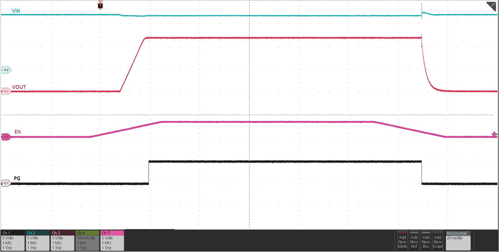
| Input supply held steady, EN/UVLO pin toggled high and low |
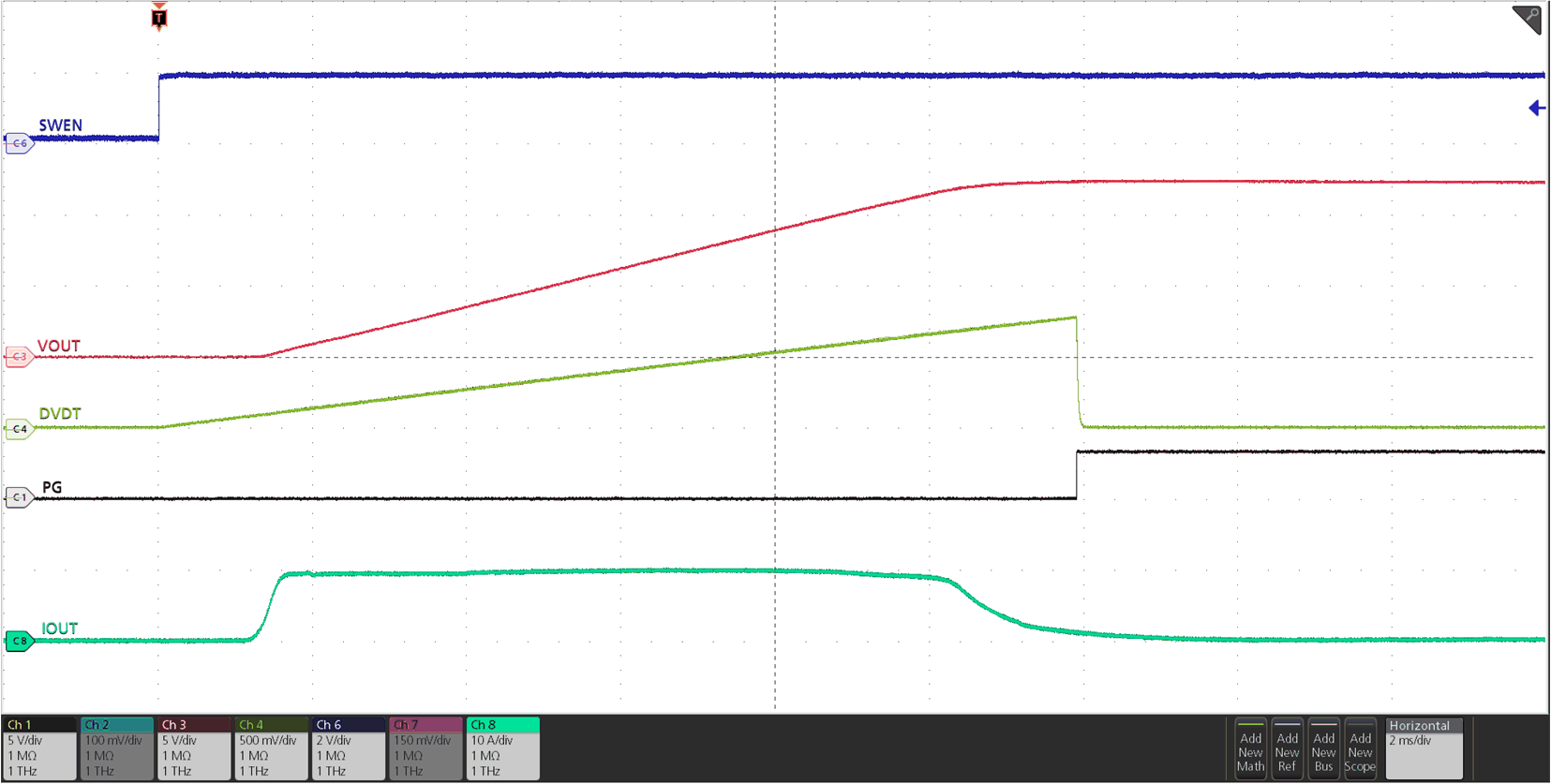
| COUT = 6.8 mF, CdVdt = 33 nF |
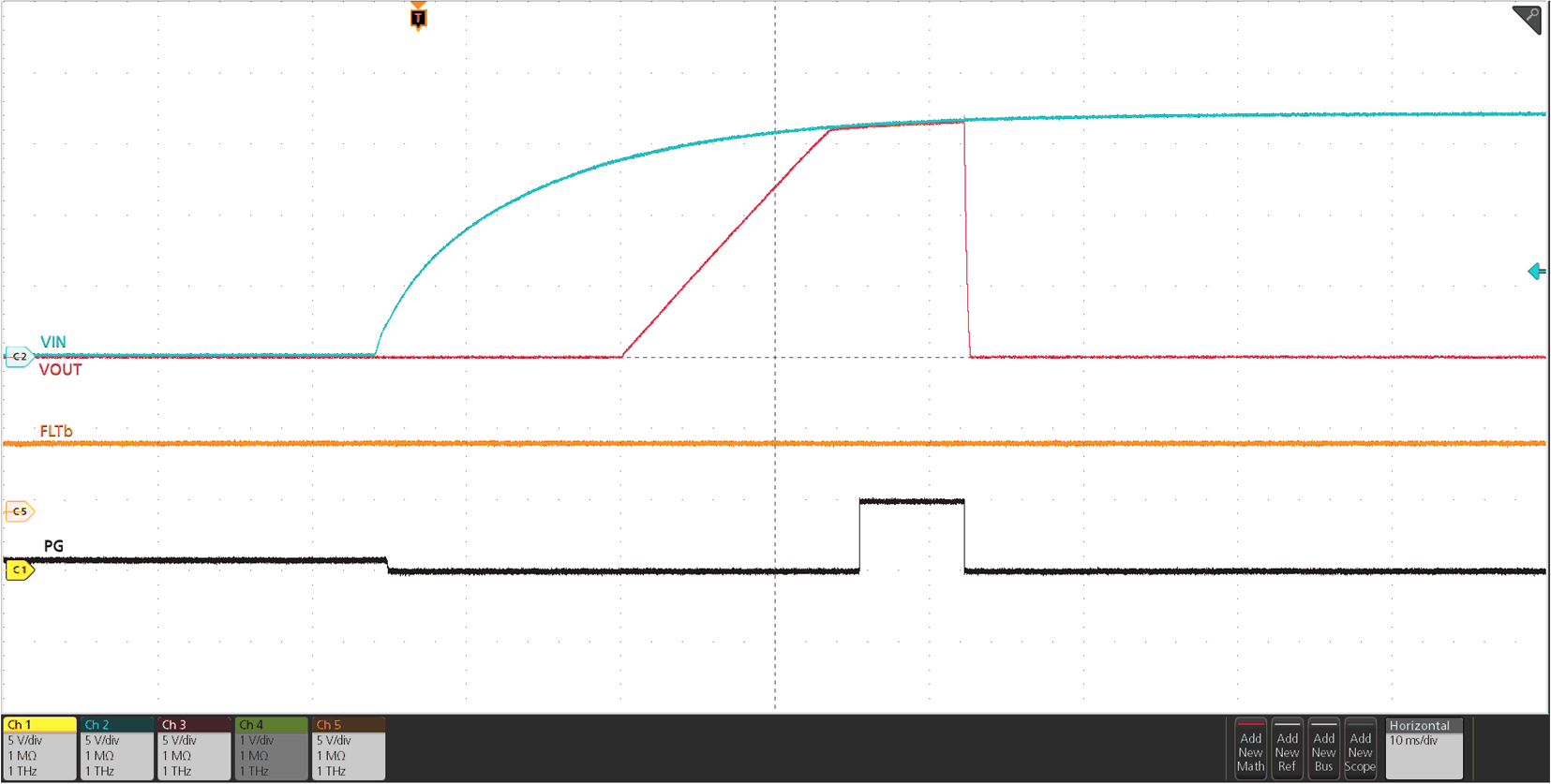
| Input supply ramped up above 16.6 V |
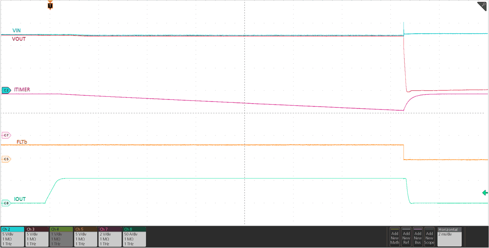
| IOCP = 50 A, tITIMER = 14 ms, IOUT stays above the IOCP threshold persistently to trigger circuit-breaker response |
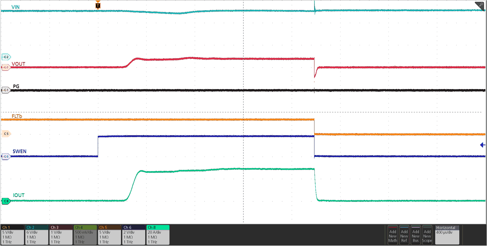
| Device turned on using SWEN with output hard-short to GND. Device limits the current with foldback. |
Figure 7-2 VDD Undervoltage
Thresholds Across Temperature
Figure 7-4 Overvoltage Protection
Threshold Across Temperature
Figure 7-6 EN/UVLO Based Shutdown
Falling Threshold Across Temperature
Figure 7-8 IMON Gain Across Load and
Temperature
Figure 7-10 IMON Gain Accuracy Across
Process and Temperature Corners
Figure 7-12 Start-up Overcurrent
Protection Threshold (Current Limit) Accuracy
Figure 7-14 Backup Overcurrent
Protection Threshold (Steady-State) Accuracy
Figure 7-16 ITIMER Pin Discharge
Current Across Temperature
Figure 7-18 SWEN Pin Logic Thresholds
Across Temperature
Figure 7-20 DVDT Gain Across
Temperature
Figure 7-22 Junction Temperature vs
Load Current (No Air-Flow)
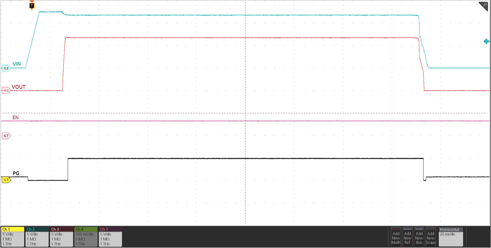
| EN held high, input supply ramped up and down |
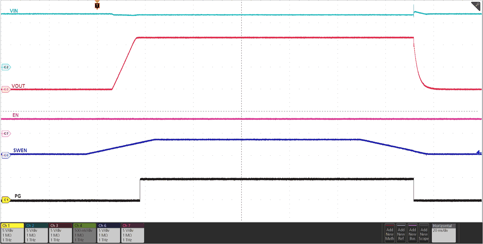
| Input supply held steady, EN/UVLO pin held high, SWEN pin toggled high and low |
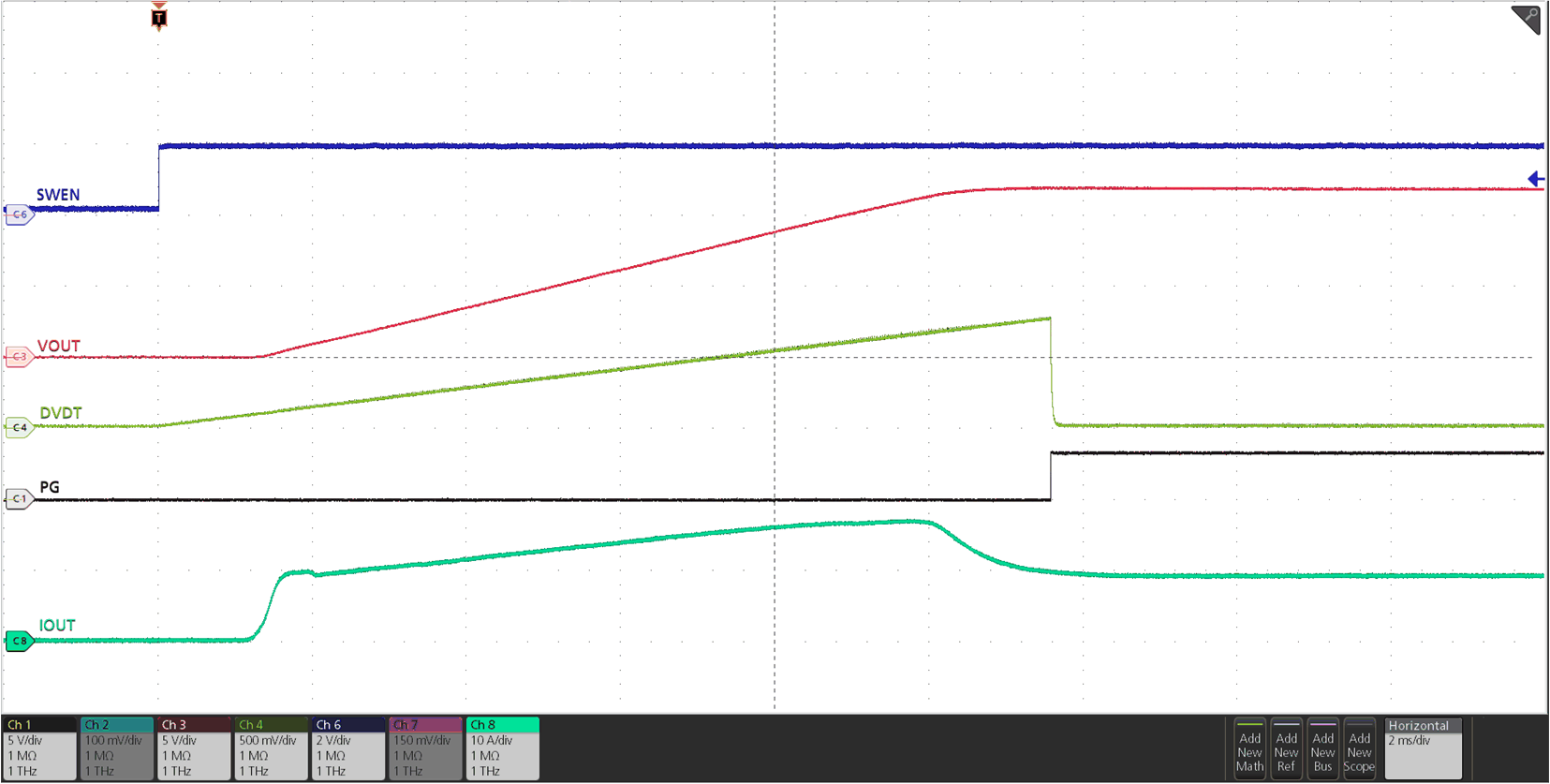
| COUT = 6.8 mF, ROUT = 1.2 Ω, CdVdt = 33 nF |
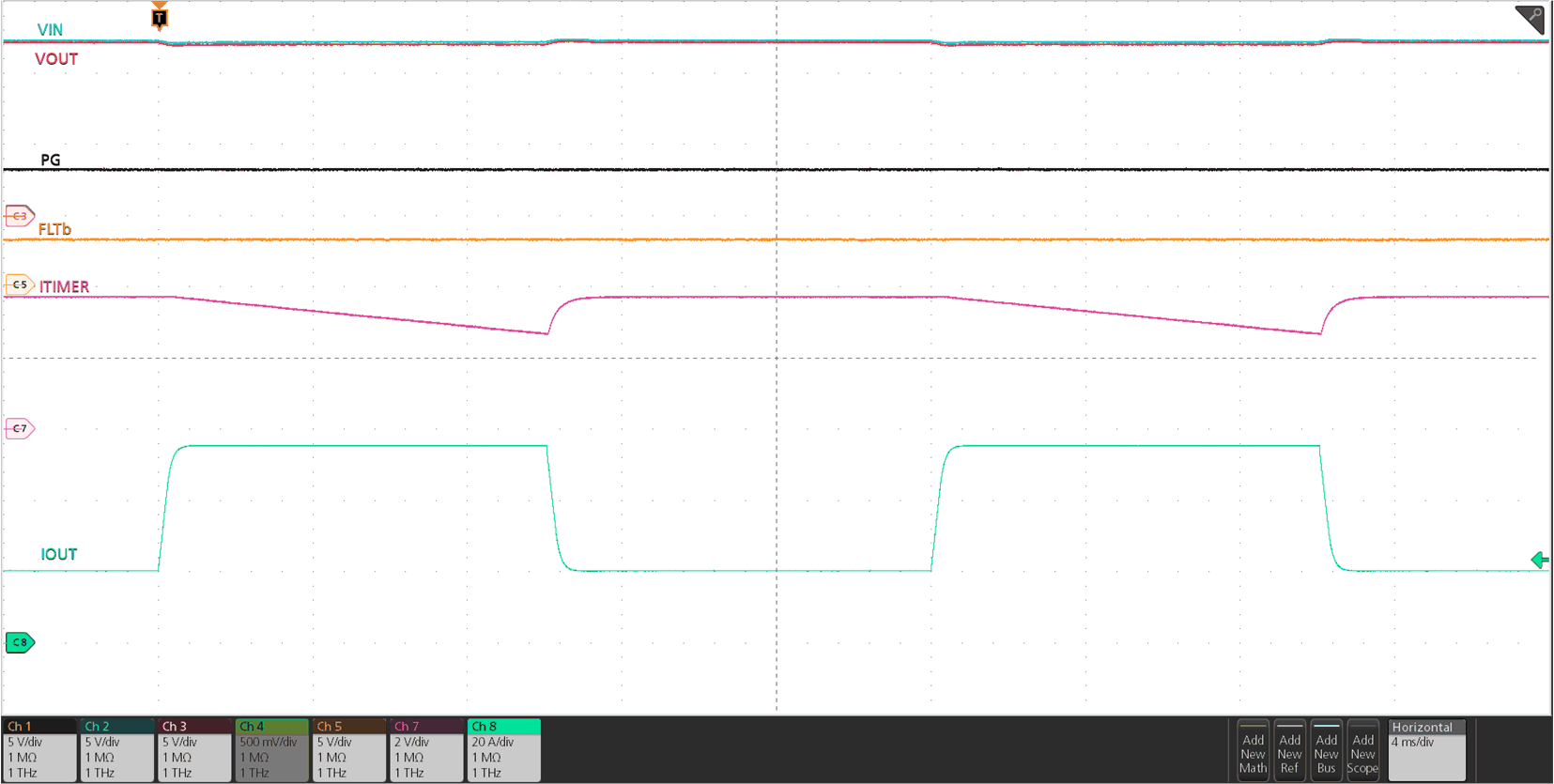
| IOCP = 50 A, tITIMER = 14 ms, IOUT pulsed above the IOCP threshold for short duration without triggering circuit-breaker response |
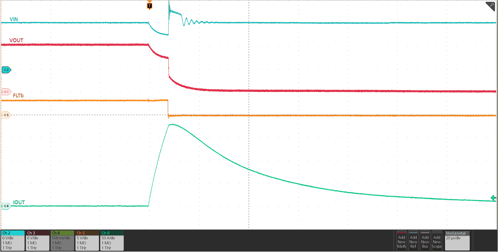
| IOCP = 50 A, Output hard-short to GND while in steady. IOUT rises above 2 × IOCP triggers fast-trip response |