ZHCSMK7C
November 2020 – December 2021
TPS2661
PRODUCTION DATA
1
特性
2
应用
3
说明
4
Revision History
5
Device Comparison Table
6
Pin Configuration and Functions
7
Specifications
7.1
Absolute Maximum Ratings
7.2
ESD Ratings
7.3
Recommended Operating Conditions
7.4
Thermal Information
7.5
Electrical Characteristics
7.6
Timing Requirements
7.7
Typical Characteristics
8
Detailed Description
8.1
Overview
8.2
Functional Block Diagram
8.3
Feature Description
8.3.1
Overload Protection and Fast-Trip
8.3.2
Reverse Current Blocking for Unipolar Current Inputs TPS26610, TPS26611 and TPS26612 (4–20 mA, 0–20 mA)
8.3.3
OUTPUT and INPUT Cutoff During Overvoltage, Undervoltage Due to Miswiring
8.3.3.1
Output Overvoltage With TPS2661x Devices
8.3.3.2
Output or Input Undervoltage With TPS26610, TPS26611 and TPS26612
8.3.3.3
Output Undervoltage With TPS26613 and TPS26614
8.3.4
External Power Supply (±Vs)
8.3.5
Loop Testing Without ±Vs Supply (Loop Power Mode in TPS26610, TPS26613 Only)
8.3.5.1
Supply Sensing With VSNS for Loop Power Mode With TPS26610 and TPS26613
8.3.6
Enable Control With TPS26611, TPS26612, and TPS26614
8.3.7
Signal Good Indicator (SGOOD)
8.4
Device Functional Modes
9
Application and Implementation
9.1
Application Information
9.2
Typical Application: Analog Input Protection for Current Inputs with TPS26610
9.2.1
Design Requirements
9.2.2
Detailed Design Procedure for Current Inputs with TPS26610
9.2.2.1
Selecting ±Vs Supplies for TPS26610
9.2.2.2
Selecting RBurden
9.2.2.3
Selecting MODE Configuration for TPS26610
9.2.3
Application Performance Plots for Current Inputs with TPS26610
9.3
Typical Application: Analog Input Protection for Multiplexed Current and Voltage Inputs with TPS26611
9.3.1
Design Requirements
9.3.2
Detailed Design Procedure for Analog Input Protection for Multiplexed Current and Voltage Inputs with TPS26611
9.3.2.1
Selecting ±Vs Supplies for TPS26611
9.3.2.2
Selecting MODE Configuration for TPS26611
9.3.2.3
Selecting Bias Resistors R1, R2 for Setting Common Mode Voltage for Voltage Inputs
9.3.3
Application Performance Plots for V/I Inputs with TPS26611
9.4
System Examples
9.4.1
Power Supply Protection of 2-Wire Transmitter with TPS26612
9.4.2
Protection of 3-Wire Transmitters and Analog Output Modules With TPS26611, TPS26612
9.4.3
UART IO Protection With TPS26611, TPS26612
9.4.4
Higher Loop Impedance With TPS26613 and TPS26614
10
Power Supply Recommendations
11
Layout
11.1
Layout Guidelines
11.2
Layout Example
12
Device and Documentation Support
12.1
接收文档更新通知
12.2
支持资源
12.3
Trademarks
12.4
Electrostatic Discharge Caution
12.5
术语表
13
Mechanical, Packaging, and Orderable Information
封装选项
机械数据 (封装 | 引脚)
DDF|8
MPDS569D
散热焊盘机械数据 (封装 | 引脚)
订购信息
zhcsmk7c_oa
zhcsmk7c_pm
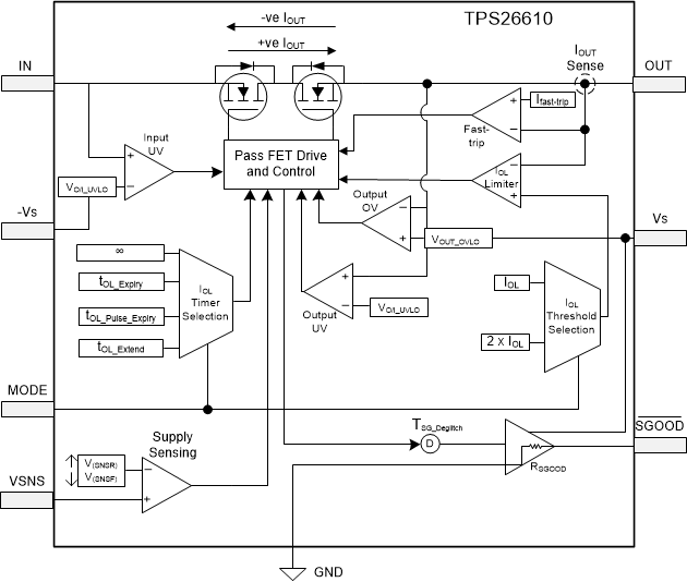
8.2
Functional Block Diagram
Figure 8-1
Functional Block Diagram for TPS26610
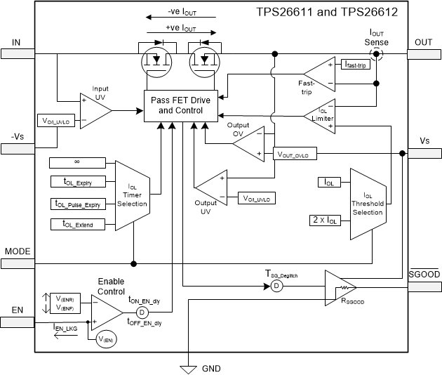
Figure 8-2
Functional Block Diagram for TPS26611 and TPS26612
Figure 8-3
Functional Block Diagram for TPS26613
Figure 8-4
Functional Block Diagram for TPS26614
千亿体育app官网登录(中国)官方网站IOS/安卓通用版/手机APP
|
米乐app下载官网(中国)|ios|Android/通用版APP最新版
|
米乐|米乐·M6(中国大陆)官方网站
|
千亿体育登陆地址
|
华体会体育(中国)HTH·官方网站
|
千赢qy国际_全站最新版千赢qy国际V6.2.14安卓/IOS下载
|
18新利网v1.2.5|中国官方网站
|
bob电竞真人(中国官网)安卓/ios苹果/电脑版【1.97.95版下载】
|
千亿体育app官方下载(中国)官方网站IOS/安卓/手机APP下载安装
|