ZHCSMK7C November   2020  – December 2021 TPS2661

PRODUCTION DATA  

  1. 特性
  2. 应用
  3. 说明
  4. Revision History
  5. Device Comparison Table
  6. Pin Configuration and Functions
  7. Specifications
    1. 7.1 Absolute Maximum Ratings
    2. 7.2 ESD Ratings
    3. 7.3 Recommended Operating Conditions
    4. 7.4 Thermal Information
    5. 7.5 Electrical Characteristics
    6. 7.6 Timing Requirements
    7. 7.7 Typical Characteristics
  8. Detailed Description
    1. 8.1 Overview
    2. 8.2 Functional Block Diagram
    3. 8.3 Feature Description
      1. 8.3.1 Overload Protection and Fast-Trip
      2. 8.3.2 Reverse Current Blocking for Unipolar Current Inputs TPS26610, TPS26611 and TPS26612 (4–20 mA, 0–20 mA)
      3. 8.3.3 OUTPUT and INPUT Cutoff During Overvoltage, Undervoltage Due to Miswiring
        1. 8.3.3.1 Output Overvoltage With TPS2661x Devices
        2. 8.3.3.2 Output or Input Undervoltage With TPS26610, TPS26611 and TPS26612
        3. 8.3.3.3 Output Undervoltage With TPS26613 and TPS26614
      4. 8.3.4 External Power Supply (±Vs)
      5. 8.3.5 Loop Testing Without ±Vs Supply (Loop Power Mode in TPS26610, TPS26613 Only)
        1. 8.3.5.1 Supply Sensing With VSNS for Loop Power Mode With TPS26610 and TPS26613
      6. 8.3.6 Enable Control With TPS26611, TPS26612, and TPS26614
      7. 8.3.7 Signal Good Indicator (SGOOD)
    4. 8.4 Device Functional Modes
  9. Application and Implementation
    1. 9.1 Application Information
    2. 9.2 Typical Application: Analog Input Protection for Current Inputs with TPS26610
      1. 9.2.1 Design Requirements
      2. 9.2.2 Detailed Design Procedure for Current Inputs with TPS26610
        1. 9.2.2.1 Selecting ±Vs Supplies for TPS26610
        2. 9.2.2.2 Selecting RBurden
        3. 9.2.2.3 Selecting MODE Configuration for TPS26610
      3. 9.2.3 Application Performance Plots for Current Inputs with TPS26610
    3. 9.3 Typical Application: Analog Input Protection for Multiplexed Current and Voltage Inputs with TPS26611
      1. 9.3.1 Design Requirements
      2. 9.3.2 Detailed Design Procedure for Analog Input Protection for Multiplexed Current and Voltage Inputs with TPS26611
        1. 9.3.2.1 Selecting ±Vs Supplies for TPS26611
        2. 9.3.2.2 Selecting MODE Configuration for TPS26611
        3. 9.3.2.3 Selecting Bias Resistors R1, R2 for Setting Common Mode Voltage for Voltage Inputs
      3. 9.3.3 Application Performance Plots for V/I Inputs with TPS26611
    4. 9.4 System Examples
      1. 9.4.1 Power Supply Protection of 2-Wire Transmitter with TPS26612
      2. 9.4.2 Protection of 3-Wire Transmitters and Analog Output Modules With TPS26611, TPS26612
      3. 9.4.3 UART IO Protection With TPS26611, TPS26612
      4. 9.4.4 Higher Loop Impedance With TPS26613 and TPS26614
  10. 10Power Supply Recommendations
  11. 11Layout
    1. 11.1 Layout Guidelines
    2. 11.2 Layout Example
  12. 12Device and Documentation Support
    1. 12.1 接收文档更新通知
    2. 12.2 支持资源
    3. 12.3 Trademarks
    4. 12.4 Electrostatic Discharge Caution
    5. 12.5 术语表
  13. 13Mechanical, Packaging, and Orderable Information

封装选项

机械数据 (封装 | 引脚)
散热焊盘机械数据 (封装 | 引脚)
订购信息

Typical Application: Analog Input Protection for Multiplexed Current and Voltage Inputs with TPS26611

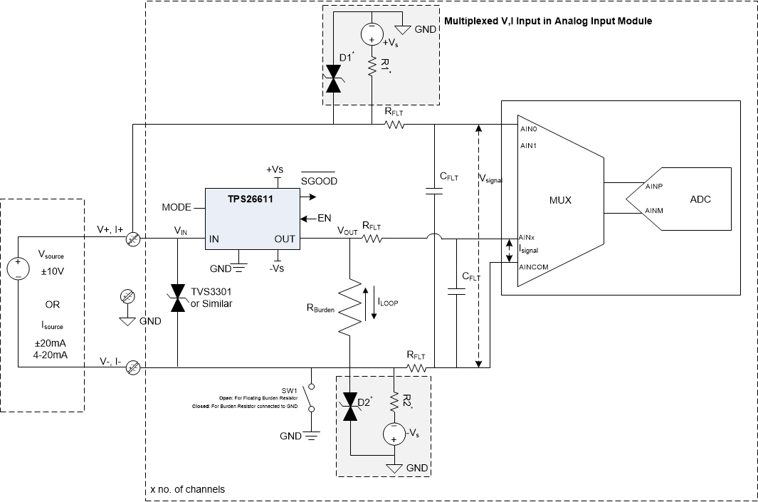
GUID-20201030-CA0I-QKK6-PQNB-2R7R9LMQNR51-low.gif Figure 9-8 Protection for Multiplexed V/I Inputs in AI Module
Bias Resistors R1*, R2* are required for setting the common mode voltage for voltage input (EN = 0) when burden resistor is floating (SW1 = Open).
Diodes D1*, D2* are required surge protection when burden resistor is floating (SW1 = Open).

TPS26611 can be used for protection of multiplexed inputs in an Analog Input module as shown in Figure 9-8. For this configuration, connect the IN pin of TPS26611 to one channel of the ADC for voltage measurement and connect OUT pin of TPS26611 to the other channel of ADC for current measurement. EN pin of TPS26611 can be used to swtch between current and voltage measurements. With EN = 0, the internal FETs of TPS26611 are turned off and voltage signal can be measured by ADC between AIN0 and AINCOM pins. Whereas with EN = 1, the internal FETs of TPS26611 are turned on and current signal can be measured by ADC between AINx and AINCOM pins.