ZHCSMK7C November 2020 – December 2021 TPS2661
PRODUCTION DATA
- 1 特性
- 2 应用
- 3 说明
- 4 Revision History
- 5 Device Comparison Table
- 6 Pin Configuration and Functions
- 7 Specifications
-
8 Detailed Description
- 8.1 Overview
- 8.2 Functional Block Diagram
- 8.3
Feature Description
- 8.3.1 Overload Protection and Fast-Trip
- 8.3.2 Reverse Current Blocking for Unipolar Current Inputs TPS26610, TPS26611 and TPS26612 (4–20 mA, 0–20 mA)
- 8.3.3 OUTPUT and INPUT Cutoff During Overvoltage, Undervoltage Due to Miswiring
- 8.3.4 External Power Supply (±Vs)
- 8.3.5 Loop Testing Without ±Vs Supply (Loop Power Mode in TPS26610, TPS26613 Only)
- 8.3.6 Enable Control With TPS26611, TPS26612, and TPS26614
- 8.3.7 Signal Good Indicator (SGOOD)
- 8.4 Device Functional Modes
-
9 Application and Implementation
- 9.1 Application Information
- 9.2 Typical Application: Analog Input Protection for Current Inputs with TPS26610
- 9.3 Typical Application: Analog Input Protection for Multiplexed Current and Voltage Inputs with TPS26611
- 9.4 System Examples
- 10Power Supply Recommendations
- 11Layout
- 12Device and Documentation Support
- 13Mechanical, Packaging, and Orderable Information
8.3.5 Loop Testing Without ±Vs Supply (Loop Power Mode in TPS26610, TPS26613 Only)
TPS26610 and TPS26613 devices allow a bipolar current limited conduction through the device even when the external +Vs/–Vs supplies are not there. When the external supply is not there, the device switches to loop power mode and derives its operating power from the 4–20-mA or ±20-mA current loop. This feature enables the field installation engineer to check the wiring of the whole current loop system by passing a test current through the current loop without actually powering on the system. This feature also helps in design of safety critical redundant systems with two redundant measurements for the same current loop. In case power is not available in one system, a second system connected in the loop is still be able to read the current information because the loop is not broken. During loop testing without ±Vs supply, the device has a voltage drop of V(IN-OUT)no_Vs, the current through device is limited to IOL_noVs. During loop testing, the device draws a current of IOL_noVs from IN pin. See the Electrical Characteristics in Specifications for V(IN-OUT)no_Vs, Iqno_Vs and IOL_noVs.
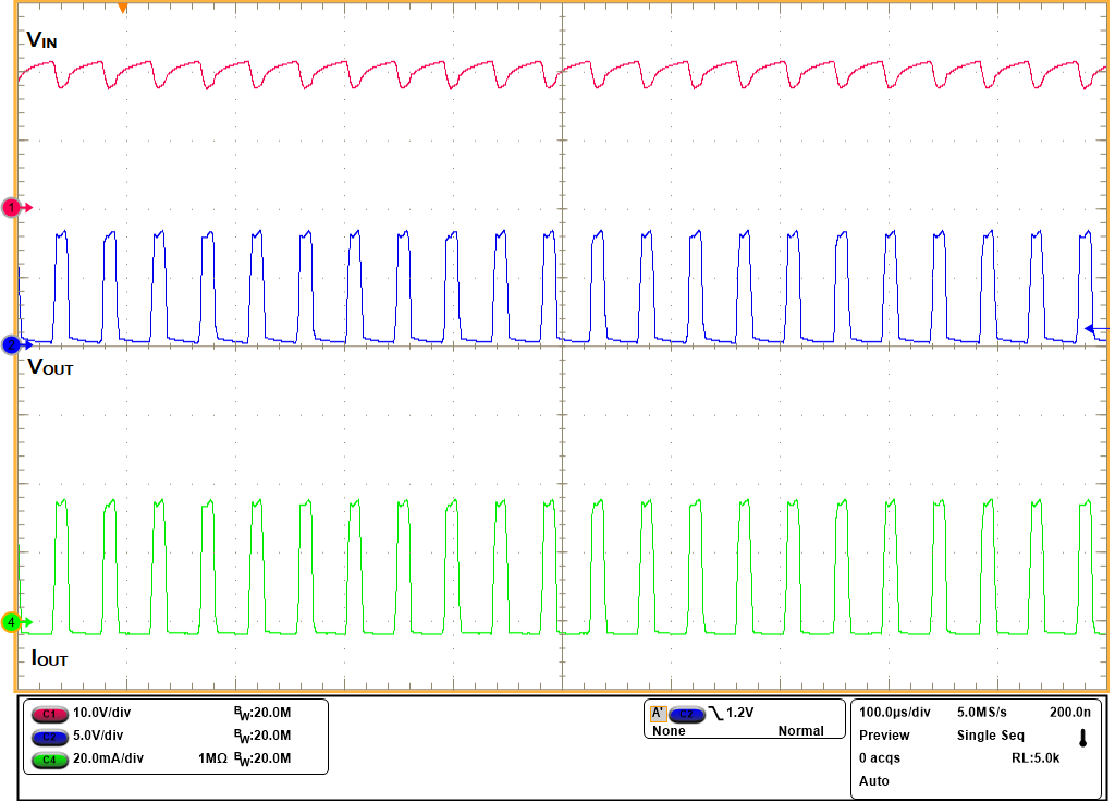
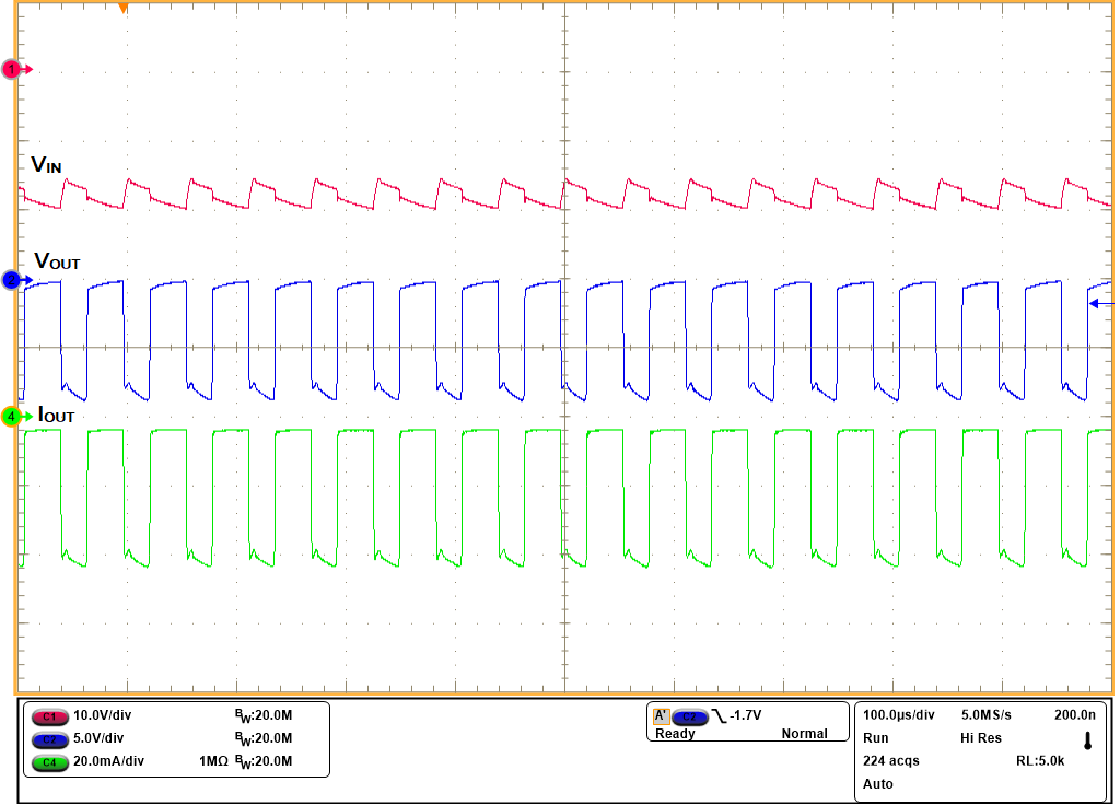
The device provides thermal protection during loop testing, if the power dissipation in device increases above 500 mW (typical), the devices turns off internal FET for short durations to limit the power dissipation. Figure 8-16 and Figure 8-17 illustrate the thermal protection during loop testing.
|
+Vs = 15 V, –Vs = –15 V, ROUT = 250 Ω, VIN = 21 V |

| +Vs = 15 V, –Vs = –15 V, ROUT = 250 Ω, VIN = –21 V |