ZHCSIU6F September 2018 – June 2021 TPS2663
PRODUCTION DATA
- 1 特性
- 2 应用
- 3 说明
- 4 Revision History
- 5 Device Comparison Table
- 6 Pin Configuration and Functions
- 7 Specifications
- 8 Parameter Measurement Information
-
9 Detailed Description
- 9.1 Overview
- 9.2 Functional Block Diagram
- 9.3
Feature Description
- 9.3.1 Hot Plug-In and In-Rush Current Control
- 9.3.2 PGOOD and PGTH
- 9.3.3 Undervoltage Lockout (UVLO)
- 9.3.4 Overvoltage Protection (OVP)
- 9.3.5 Input Reverse Polarity Protection (B_GATE, DRV)
- 9.3.6 Reverse Current Protection
- 9.3.7 Overload and Short Circuit Protection
- 9.3.8 Output Power Limiting, PLIM (TPS26632, TPS26633, TPS26635 and TPS26636 Only)
- 9.3.9 Current Monitoring Output (IMON)
- 9.3.10 FAULT Response ( FLT)
- 9.3.11 IN_SYS, IN, OUT and GND Pins
- 9.3.12 Thermal Shutdown
- 9.3.13 Low Current Shutdown Control (SHDN)
- 9.4 Device Functional Modes
-
10Application and Implementation
- 10.1 Application Information
- 10.2
Typical Application: Power Path Protection in a PLC System
- 10.2.1 Design Requirements
- 10.2.2 Detailed Design Procedure
- 10.2.3 Application Curves
- 10.3 System Examples
- 10.4 Do's and Don'ts
- 11Power Supply Recommendations
- 12Layout
- 13Device and Documentation Support
- 14Mechanical, Packaging, and Orderable Information
10.3.1 Simple 24-V Power Supply Path Protection
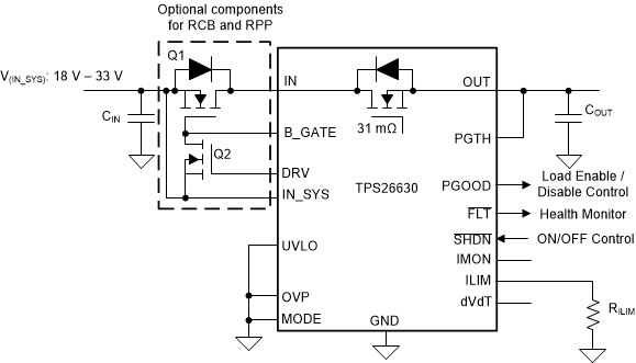
With the TPS2663x devices, a simple 24-V power supply path protection can be realized using a minimum of five external components as shown in the schematic diagram in Figure 10-11. The external components required are: a N–Channel Power FET Q1, a N–Channel signal FET Q2 and a R(ILIM) resistor to program the current limit, C(IN) and C(OUT) capacitors.
 Figure 10-11 TPS26630 Configured for a Simple 24-V Supply Path Protection
Protection features with this configuration include:
- Load and device protection from reverse input polarity fault down to –60 V (with a 60-V rated Q1)
- Overvoltage Protection at 34 V
- Inrush current control with 24-V/240-µs output voltage slew rate
- Reverse Current Blocking
- Accurate current limiting with Auto-Retry