ZHCSIU6F September 2018 – June 2021 TPS2663
PRODUCTION DATA
- 1 特性
- 2 应用
- 3 说明
- 4 Revision History
- 5 Device Comparison Table
- 6 Pin Configuration and Functions
- 7 Specifications
- 8 Parameter Measurement Information
-
9 Detailed Description
- 9.1 Overview
- 9.2 Functional Block Diagram
- 9.3
Feature Description
- 9.3.1 Hot Plug-In and In-Rush Current Control
- 9.3.2 PGOOD and PGTH
- 9.3.3 Undervoltage Lockout (UVLO)
- 9.3.4 Overvoltage Protection (OVP)
- 9.3.5 Input Reverse Polarity Protection (B_GATE, DRV)
- 9.3.6 Reverse Current Protection
- 9.3.7 Overload and Short Circuit Protection
- 9.3.8 Output Power Limiting, PLIM (TPS26632, TPS26633, TPS26635 and TPS26636 Only)
- 9.3.9 Current Monitoring Output (IMON)
- 9.3.10 FAULT Response ( FLT)
- 9.3.11 IN_SYS, IN, OUT and GND Pins
- 9.3.12 Thermal Shutdown
- 9.3.13 Low Current Shutdown Control (SHDN)
- 9.4 Device Functional Modes
-
10Application and Implementation
- 10.1 Application Information
- 10.2
Typical Application: Power Path Protection in a PLC System
- 10.2.1 Design Requirements
- 10.2.2 Detailed Design Procedure
- 10.2.3 Application Curves
- 10.3 System Examples
- 10.4 Do's and Don'ts
- 11Power Supply Recommendations
- 12Layout
- 13Device and Documentation Support
- 14Mechanical, Packaging, and Orderable Information
9.3.8 Output Power Limiting, PLIM (TPS26632, TPS26633, TPS26635 and TPS26636 Only)
The TPS26630 and TPS26631 devices with a fixed overcurrent limit threshold the maximum output power limit increases linearly with supply input. Electrical industrial process control equipment such as PLC CPU needs to comply with standards like IEC61010-1 and UL1310 for fire safety, which require limited energy and power circuits. Limiting the output power becomes a challenge in such high power applications where the operating supply voltage range is wide. The TPS26632, TPS26633, TPS26635 and TPS26636 devices integrate adjustable output power limiting functionality that simplifies the system design requiring compliance in accordance to this standard.
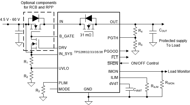
Connect a resistor from PLIM to GND as shown in Figure 9-16 to set the output power limiting value. If output power limiting is not required then connect PLIM to GND directly. This disables the PLIM functionality.
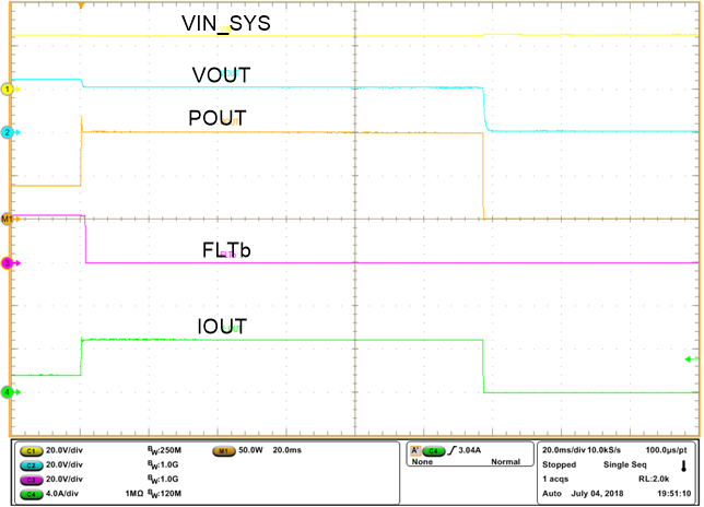
During an over power load event the TPS26632 limits the output power at the programmed value set by PLIM resistor. This indirectly results in the device operation in current limiting mode with steady state output voltage and current set by the load characteristics and PLIM = VOUT × IOUT. Figure 7-12 shows the output power limit and current limit characteristics of TPS26632 with 100 W power limit setting. The maximum duration for the device in power limiting mode is 162 msec (typical), tCL_PLIM(dly). After this time, the device operates either in auto-retry or latch off mode based on MODE pin configuration in Table 9-1.
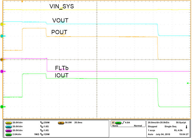
During an over power load event the TPS26633, TPS26635 and TPS26636 allows the extra power for a maximum duration of tCB(dly), 25.5 msec (typical). The maximum power during this time is limited to VOUT x 2 x IOL where IOL is the overload current limit set by the R(ILIM) resistor. After the tCB(dly) time, the output power gets limited to the value programmed by the PLIM resistor. Set the power limit using Equation 6.
Here P(PLIM) is output power limit in watts, R(PLIM) is the power limit setting resistor in kΩ. Figure 9-17 and Figure 9-18 illustrate output power limiting performance of TPS26632 and TPS26633 devices respectively.
Refer to Figure 8-2 for more information on tCB(dly) and tCL_PLIM(dly) parameter measurement information.
 Figure 9-16 TPS26632, TPS26633, TPS26635 and TPS26636 Typical Application Schematic
| RPLIM = 100 kΩ | RILIM = 3 kΩ |

| RPLIM = 100 kΩ | RILIM = 3 kΩ |