SLVSH67 September   2024 TPS26750

PRODUCTION DATA  

  1.   1
  2. Features
  3. Applications
  4. Description
  5. Pin Configuration and Functions
  6. Specifications
    1. 5.1  Absolute Maximum Ratings
      1. 5.1.1 TPS26750 - Absolute Maximum Ratings
      2. 5.1.2 TPS26750 - Absolute Maximum Ratings
    2. 5.2  ESD Ratings
    3. 5.3  Recommended Operating Conditions
      1. 5.3.1 TPS26750 - Recommended Operating Conditions
    4. 5.4  Recommended Capacitance
    5. 5.5  Thermal Information
      1. 5.5.1 TPS26750 - Thermal Information
    6. 5.6  Power Supply Characteristics
    7. 5.7  Power Consumption
    8. 5.8  PP_5V Power Switch Characteristics
    9. 5.9  POWER_PATH_EN Characteristics - TPS26750
    10. 5.10 Power Path Supervisory
    11. 5.11 CC Cable Detection Parameters
    12. 5.12 CC VCONN Parameters
    13. 5.13 CC PHY Parameters
    14. 5.14 Thermal Shutdown Characteristics
    15. 5.15 ADC Characteristics
    16. 5.16 Input/Output (I/O) Characteristics
    17. 5.17 BC1.2 Characteristics
    18. 5.18 I2C Requirements and Characteristics
    19. 5.19 Typical Characteristics
  7. Parameter Measurement Information
  8. Detailed Description
    1. 7.1 Overview
    2. 7.2 Functional Block Diagram
    3. 7.3 Feature Description
      1. 7.3.1  USB-PD Physical Layer
        1. 7.3.1.1 USB-PD Encoding and Signaling
        2. 7.3.1.2 USB-PD Bi-Phase Marked Coding
        3. 7.3.1.3 USB-PD Transmit (TX) and Receive (Rx) Masks
        4. 7.3.1.4 USB-PD BMC Transmitter
        5. 7.3.1.5 USB-PD BMC Receiver
        6. 7.3.1.6 Squelch Receiver
      2. 7.3.2  Power Management
        1. 7.3.2.1 Power-On And Supervisory Functions
        2. 7.3.2.2 VBUS LDO
      3. 7.3.3  Power Paths
        1. 7.3.3.1 Internal Sourcing Power Paths
          1. 7.3.3.1.1 PP_5V Current Clamping
          2. 7.3.3.1.2 PP_5V Local Overtemperature Shut Down (OTSD)
          3. 7.3.3.1.3 PP_5V OVP
          4. 7.3.3.1.4 PP_5V UVLO
          5. 7.3.3.1.5 PP_5Vx Reverse Current Protection
          6. 7.3.3.1.6 PP_CABLE Current Clamp
          7. 7.3.3.1.7 PP_CABLE Local Overtemperature Shut Down (OTSD)
          8. 7.3.3.1.8 PP_CABLE UVLO
      4. 7.3.4  Cable Plug and Orientation Detection
        1. 7.3.4.1 Configured as a Source
        2. 7.3.4.2 Configured as a Sink
        3. 7.3.4.3 Configured as a DRP
        4. 7.3.4.4 Dead Battery Advertisement
      5. 7.3.5  Overvoltage Protection (CC1, CC2)
      6. 7.3.6  Default Behavior Configuration (ADCIN1, ADCIN2)
      7. 7.3.7  ADC
      8. 7.3.8  BC 1.2 (USB_P, USB_N)
      9. 7.3.9  Digital Interfaces
        1. 7.3.9.1 General GPIO
        2. 7.3.9.2 I2C Interface
      10. 7.3.10 Digital Core
      11. 7.3.11 I2C Interface
        1. 7.3.11.1 I2C Interface Description
          1. 7.3.11.1.1 I2C Clock Stretching
          2. 7.3.11.1.2 I2C Address Setting
          3. 7.3.11.1.3 Unique Address Interface
    4. 7.4 Device Functional Modes
      1. 7.4.1 Pin Strapping to Configure Default Behavior
      2. 7.4.2 Power States
    5. 7.5 Thermal Shutdown
  9. Application and Implementation
    1. 8.1 Application Information
    2. 8.2 Typical Application
      1. 8.2.1 Design Requirements
        1. 8.2.1.1 Programmable Power Supply (PPS) - Design Requirements
        2. 8.2.1.2 Liquid Detection Design Requirements
        3. 8.2.1.3 BC1.2 Application Design Requirements
        4. 8.2.1.4 USB Data Support Design Requirements
        5. 8.2.1.5 EPR Design Requirements
      2. 8.2.2 Detailed Design Procedure
        1. 8.2.2.1 Programmable Power Supply (PPS)
        2. 8.2.2.2 Liquid Detection
        3. 8.2.2.3 BC1.2 Application
        4. 8.2.2.4 USB Data Support
        5. 8.2.2.5 Power Delivery EPR Support
      3. 8.2.3 Application Curves
        1. 8.2.3.1 Programmable Power Supply (PPS) Application Curves
        2. 8.2.3.2 Liquid Detection Application Curves
        3. 8.2.3.3 BC1.2 Application Curves
        4. 8.2.3.4 USB Data Support Application Curves
        5. 8.2.3.5 EPR Application Curves
    3. 8.3 Power Supply Recommendations
      1. 8.3.1 3.3V Power
        1. 8.3.1.1 VIN_3V3 Input Switch
      2. 8.3.2 1.5V Power
      3. 8.3.3 Recommended Supply Load Capacitance
    4. 8.4 Layout
      1. 8.4.1 TPS26750 - Layout
        1. 8.4.1.1 Layout Guidelines
          1. 8.4.1.1.1 Recommended Via Size
          2. 8.4.1.1.2 Minimum Trace Widths
        2. 8.4.1.2 Layout Example
          1. 8.4.1.2.1 TPS26750 Schematic Layout Example
          2. 8.4.1.2.2 TPS26750 Layout Example - PCB Plots
            1. 8.4.1.2.2.1 TPS26750 Component Placement
            2. 8.4.1.2.2.2 TPS26750 PP5V
            3. 8.4.1.2.2.3 TPS26750 PP_EXT
            4. 8.4.1.2.2.4 TPS26750 VBUS
            5. 8.4.1.2.2.5 TPS26750 I/O
            6. 8.4.1.2.2.6 TPS26750 PPEXT Gate Driver
            7. 8.4.1.2.2.7 TPS26750 GND
  10. Device and Documentation Support
    1. 9.1 Device Support
      1. 9.1.1 Third-Party Products Disclaimer
    2. 9.2 Documentation Support
      1. 9.2.1 Related Documentation
    3. 9.3 Support Resources
    4. 9.4 Trademarks
    5. 9.5 Electrostatic Discharge Caution
    6. 9.6 Glossary
  11. 10Revision History
  12. 11Mechanical, Packaging, and Orderable Information

封装选项

请参考 PDF 数据表获取器件具体的封装图。

机械数据 (封装 | 引脚)
  • RSM|32
散热焊盘机械数据 (封装 | 引脚)
订购信息

USB-PD BMC Transmitter

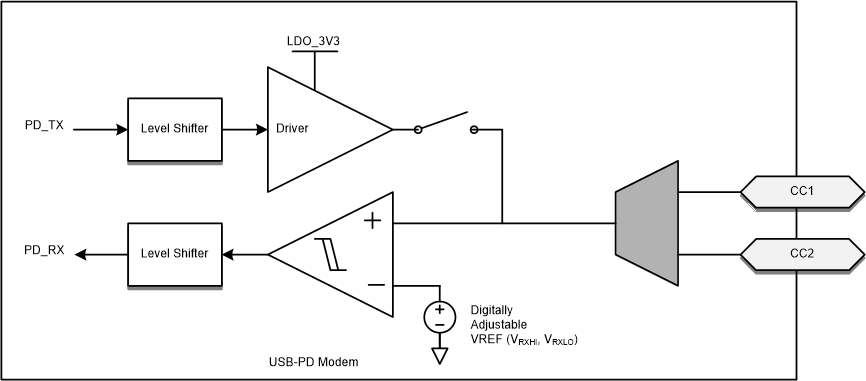
The TPS26750 transmits and receives USB-PD data over one of the CCy pins for a given CC pin pair (one pair per USB Type-C port). The CCy pins are also used to determine the cable orientation and maintain the cable/device attach detection. Thus, a DC bias exists on the CCy pins. The transmitter driver overdrives the CCy DC bias while transmitting, but returns to a Hi-Z state, allowing the DC voltage to return to the CCy pin when it is not transmitting. While either CC1 or CC2 can be used for transmitting and receiving, during a given connection only, the one that mates with the CC pin of the plug is used, so there is no dynamic switching between CC1 and CC2. Figure 7-5 shows the USB-PD BMC TX and RX driver block diagram.
TPS26750 USB-PD
                    BMC TX/Rx Block Diagram Figure 7-5 USB-PD BMC TX/Rx Block Diagram

Figure 7-6 shows the transmission of the BMC data on top of the DC bias. Note that the DC bias can be anywhere between the minimum and maximum threshold for detecting a Sink attach. This note means that the DC bias can be above or below the VOH of the transmitter driver.
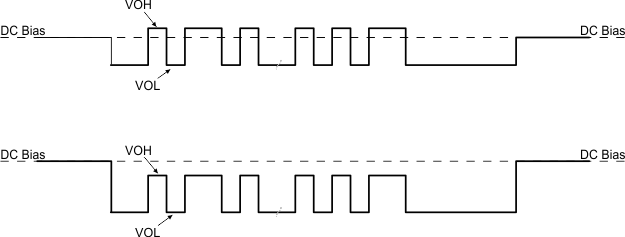
TPS26750 TX Driver Transmission with DC BiasFigure 7-6 TX Driver Transmission with DC Bias

The transmitter drives a digital signal onto the CCy lines. The signal peak, VTXHI, is set to meet the TX masks defined in the USB-PD Specifications. Note that the TX mask is measured at the far-end of the cable.

When driving the line, the transmitter driver has an output impedance of ZDRIVER. ZDRIVER is determined by the driver resistance and the shunt capacitance of the source and is frequency dependent. ZDRIVER impacts the noise ingression in the cable.

Figure 7-7 shows the simplified circuit determining ZDRIVER. It is specified such that noise at the receiver is bounded.

TPS26750 ZDRIVER CircuitFigure 7-7 ZDRIVER Circuit