SLVSBE9E April 2012 – June 2015 TPS27081A
PRODUCTION DATA.
- 1 Features
- 2 Applications
- 3 Description
- 4 Revision History
- 5 Pin Configuration and Functions
- 6 Specifications
- 7 Detailed Description
-
8 Application and Implementation
- 8.1 Application Information
- 8.2 Typical Application
- 8.3
System Examples
- 8.3.1 Standby Power Isolation
- 8.3.2 Boost Regulator With True Shutdown
- 8.3.3 Single Module Multiple Power Supply Sequencing
- 8.3.4 Multiple Modules Interdependent Power Supply Sequencing
- 8.3.5 TFT LCD Module Inrush Current Control
- 8.3.6 Multiple Modules Interdependent Supply Sequencing Without a GPIO Input
- 9 Power Supply Recommendations
- 10Layout
- 11Device and Documentation Support
- 12Mechanical, Packaging, and Orderable Information
7 Detailed Description
7.1 Overview
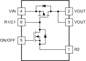
The TPS27081A device is a load switch capable fo handing up to 8 V and 3 A. To reduce voltage drop for low voltage and high current rails, the device implements an ultra-low resistance P-channel MOSFET which reduces the dropout voltage through the device.
The device has a programmable slew rate which helps reduce or eliminate power supply droop due to large inrush currents. During shutdown, the device has very low leakage currents.
7.2 Functional Block Diagram

7.3 Feature Description
The TPS27081A device uses a low-voltage power PMOS transistor used as the pass element or switch between the supply and load. The device also uses an NMOS transistor to turn the PMOS on and off by interfacing with a wide range of GPIO voltages. Asserting an input voltage higher than VIH (1 V) enables the PMOS switch by turning the NMOS and the NMOS driving the PMOS gate towards ground. When using R2 to control output rise time and a pullup resistor R1 to tie the gate of the PMOS to the source to ensure turnoff, be sure to use an R1 value big enough to source a small enough of current into R2 to not grossly effect the PMOS ON-state gate voltage.
TPS27081A offers additional ports to control the output rise time by connecting passive elements between these pins, VIN, and VOUT.
7.4 Device Functional Modes
7.4.1 ON/OFF
When VIN > approximately 1 V and V(ON/OFF) > 1 V, the switch turns on and VOUT ≈ VIN.
When VIN > approximately 1 V and V(ON/OFF) <1 V, the switch turns off and VOUT ≠ VIN.
7.4.2 Fastest Output Rise Time
Whenever it is desired to achieve the fastest output rise time, tie pin 1 (R2) to ground and do not put a capacitor between VOUT (pins 2 and 3) and R1 and C1 (pin 6).
7.4.3 Controlled Output Rise Time
Whenever it is desired to control the output rise time, tie pin 1 (R2) to a resistance (R2) and put a capacitor (C1) between VOUT (pins 2 and 3) and R1 and C1 (pin 6). The values needed to determine a certain output rise time can be determined by Equation 3.