SLVSBE9E April 2012 – June 2015 TPS27081A
PRODUCTION DATA.
- 1 Features
- 2 Applications
- 3 Description
- 4 Revision History
- 5 Pin Configuration and Functions
- 6 Specifications
- 7 Detailed Description
-
8 Application and Implementation
- 8.1 Application Information
- 8.2 Typical Application
- 8.3
System Examples
- 8.3.1 Standby Power Isolation
- 8.3.2 Boost Regulator With True Shutdown
- 8.3.3 Single Module Multiple Power Supply Sequencing
- 8.3.4 Multiple Modules Interdependent Power Supply Sequencing
- 8.3.5 TFT LCD Module Inrush Current Control
- 8.3.6 Multiple Modules Interdependent Supply Sequencing Without a GPIO Input
- 9 Power Supply Recommendations
- 10Layout
- 11Device and Documentation Support
- 12Mechanical, Packaging, and Orderable Information
10 Layout
10.1 Layout Guidelines
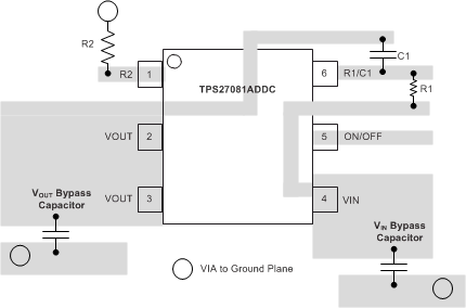
For best operational performance of the device, use good PCB layout practices, including:
- VIN and VOUT traces should be as short and wide as possible to accommodate for high current.
- The VIN pin should be bypassed to ground with low ESR ceramic bypass capacitors. The typical recommended bypass capacitance is 1-μF ceramic with X5R or X7R dielectric. This capacitor should be placed as close to the device pins as possible.
- The VOUT pin should be bypassed to ground with low ESR ceramic bypass capacitors. The typical recommended bypass capacitance is one-tenth of the VIN bypass capacitor of X5R or X7R dielectric rating. This capacitor should be placed as close to the device pins as possible.
10.2 Layout Example
 Figure 23. Layout Example
10.3 Thermal Reliability
For higher reliability, TI recommends limiting the TPS27081A die junction temperature to less than 105°C. The device junction temperature is directly proportional to the ON-chip power dissipation. Use the following equation to calculate maximum ON-chip power dissipation to achieve the maximum die junction temperature target:

where
- TJ(max) is the target maximum junction temperature
- TA is the operating ambient temperature
- RθJA is the package junction to ambient thermal resistance
10.4 Improving Package Thermal Performance
The package RθJA value under standard conditions on a High-K board is listed in . RθJA value depends on the PC board layout. An external heat sink and/or a cooling mechanism, like a cold air fan, can help reduce RθJA and thus improve device thermal capabilities. Refer to TI’s design support web page at www.ti.com/thermal for a general guidance on improving device thermal performance.