ZHCSMM1C April 2023 – February 2024 TPS274C65
PRODUCTION DATA
- 1
- 1 特性
- 2 应用
- 3 说明
- 4 Device Comparison Table
- 5 Pin Configuration and Functions
- 6 Specifications
- 7 Parameter Measurement Information
-
8 Detailed Description
- 8.1 Overview
- 8.2 Functional Block Diagram
- 8.3
Feature Description
- 8.3.1 Pin Diagrams
- 8.3.2 SPI Mode Operation
- 8.3.3 Programmable Current Limit
- 8.3.4 DO_EN Feature
- 8.3.5
Protection Mechanisms
- 8.3.5.1 Overcurrent Protection
- 8.3.5.2 Short Circuit Protection
- 8.3.5.3 Inductive-Load Switching-Off Clamp
- 8.3.5.4 Inductive Load Demagnetization
- 8.3.5.5 Thermal Shutdown
- 8.3.5.6 Undervoltage protection on VS
- 8.3.5.7 Undervoltage Lockout on Low Voltage Supply (VDD_UVLO)
- 8.3.5.8 Power-Up and Power-Down Behavior
- 8.3.5.9 Reverse Current Blocking
- 8.3.6 Diagnostic Mechanisms
- 8.3.7 LED Driver
- 8.4 Device Functional Modes
- 8.5 TPS274C65BS Available Registers List
- 8.6 TPS274C65 Registers
- 9 Application and Implementation
- 10Device and Documentation Support
- 11Revision History
- 12Mechanical, Packaging, and Orderable Information
8.3.5.4 Inductive Load Demagnetization
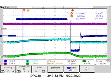
When switching off an inductive load, the inductor can impose a negative voltage on the output of the switch. The TPS274C65 includes voltage clamps between VS and VOUT to limit the voltage across the FETs and demagnetize load inductance if there is any. The negative voltage applied at the OUT pin drives the discharge of inductor current. Figure 8-26 shows the device discharging a load of 100mH paralleled with 48Ω, resulting 500mA at the turn-off.
 Figure 8-26 TPS274C65 Inductive Discharge (100mH +
48Ω)
Figure 8-26 TPS274C65 Inductive Discharge (100mH +
48Ω)The maximum acceptable load inductance is a function of the energy dissipated in the device and therefore the load current and the inductive load. The maximum energy and the load inductance the device can withstand for one pulse inductive dissipation at 125°C is shown in Figure 8-27. The device can withstand 40% of this energy for one million inductive repetitive pulses with a 2Hz repetitive pulse. If the application parameters exceed this device limit, use a protection device like a freewheeling diode to dissipate the energy stored in the inductor.
 Figure 8-27 Maximum Energy Dissipation
(EAS) Allowed TJ, START = 125°C – Single Pulse, One
Channel