ZHCSHQ0B October 2017 – September 2019 TPS27S100
PRODUCTION DATA.
- 1 特性
- 2 应用
- 3 说明
- 4 修订历史记录
- 5 Pin Configuration and Functions
- 6 Specifications
- 7 Detailed Description
- 8 Application and Implementation
- 9 Power Supply Recommendations
- 10Layout
- 11器件和文档支持
- 12机械、封装和可订购信息
封装选项
机械数据 (封装 | 引脚)
散热焊盘机械数据 (封装 | 引脚)
- PWP|14
订购信息
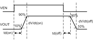
6.7 Switching Characteristics
VIN = 24 V, Rload = 24 Ω, over operating free-air temperature range (unless otherwise noted)(1)| PARAMETER | TEST CONDITIONS | MIN | TYP | MAX | UNIT | |
|---|---|---|---|---|---|---|
| td(on) | Turn-on delay time | EN rising edge to VOUT = 10%, DIAG_EN high | 20 | 50 | µs | |
| td(off) | Turn-off delay time | EN falling edge to VOUT = 90%, DIAG_EN high | 40 | 80 | µs | |
| dV/dt(on) | Slew rate on | VOUT = 10% to 90%, DIAG_EN high | 0.1 | 0.5 | V/µs | |
| dV/dt(off) | Slew rate off | VOUT = 90% to 10%, DIAG_EN high | 0.1 | 0.5 | V/µs | |
(1) Value specified by design, not subject to production test.
Figure 1. Pin Current and Voltage Conventions
 Figure 2. Output Delay Characteristics
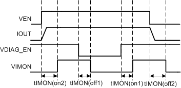
  Figure 3. Current sense Delay Characteristics
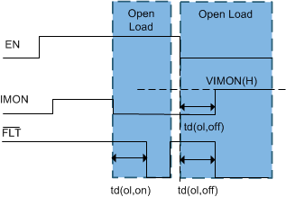
  Figure 4. Open Load Blanking Time Characteristics