ZHCSMM0 December   2020 TPS27SA08-Q1

PRODUCTION DATA  

  1. 特性
  2. 应用
  3. 说明
  4. Revision History
  5. Device Summary Table
  6. Pin Configuration and Functions
    1. 6.1 Recommended Connections for Unused Pins
  7. Specifications
    1. 7.1 Absolute Maximum Ratings
    2. 7.2 ESD Ratings
    3. 7.3 Recommended Operating Conditions
    4. 7.4 Thermal Information
    5. 7.5 Electrical Characteristics
    6. 7.6 Switching Characteristics
    7. 7.7 SNS Timing Characteristics
    8. 7.8 Typical Characteristics
  8. Parameter Measurement Information
  9. Detailed Description
    1. 9.1 Overview
    2. 9.2 Functional Block Diagram
    3. 9.3 Feature Description
      1. 9.3.1 Protection Mechanisms
        1. 9.3.1.1 Thermal Shutdown
        2. 9.3.1.2 Current Limit
          1. 9.3.1.2.1 Current Limit Foldback
          2. 9.3.1.2.2 Undervoltage Lockout (UVLO)
          3. 9.3.1.2.3 VBB during Short-to-Ground
        3. 9.3.1.3 Energy Limit
        4. 9.3.1.4 Voltage Transients
          1. 9.3.1.4.1 Driving Inductive and Capacitive Loads
        5. 9.3.1.5 Reverse supply
        6. 9.3.1.6 Fault Event – Timing Diagrams
      2. 9.3.2 Diagnostic Mechanisms
        1. 9.3.2.1 VOUT Short-to-supply and Open-Load
          1. 9.3.2.1.1 Detection With Switch Enabled
          2. 9.3.2.1.2 Detection With Switch Disabled
        2. 9.3.2.2 SNS Output
          1. 9.3.2.2.1 RSNS Value
            1. 9.3.2.2.1.1 High Accuracy Load Current Sense
            2. 9.3.2.2.1.2 SNS Output Filter
        3. 9.3.2.3 ST Pin
        4. 9.3.2.4 Fault Indication and SNS Mux
        5. 9.3.2.5 Resistor Sharing
        6. 9.3.2.6 High-Frequency, Low Duty-Cycle Current Sensing
    4. 9.4 Device Functional Modes
      1. 9.4.1 Off
      2. 9.4.2 Standby
      3. 9.4.3 Diagnostic
      4. 9.4.4 Standby Delay
      5. 9.4.5 Active
      6. 9.4.6 Fault
  10. 10Application and Implementation
    1. 10.1 Application Information
      1. 10.1.1 Ground Protection Network
      2. 10.1.2 Interface With Microcontroller
      3. 10.1.3 I/O Protection
      4. 10.1.4 Inverse Current
      5. 10.1.5 Loss of GND
      6. 10.1.6 Thermal Information
    2. 10.2 Typical Application
      1. 10.2.1 Design Requirements
      2. 10.2.2 Detailed Design Procedure
        1. 10.2.2.1 Thermal Considerations
        2. 10.2.2.2 Diagnostics
          1. 10.2.2.2.1 Selecting the RISNS Value
      3. 10.2.3 Application Curves
  11. 11Power Supply Recommendations
  12. 12Layout
    1. 12.1 Layout Guidelines
    2. 12.2 Layout Example
  13. 13Device and Documentation Support
    1. 13.1 Device Support
      1. 13.1.1 Related Documentation
    2. 13.2 Trademarks
    3. 13.3 Electrostatic Discharge Caution
    4. 13.4 Glossary
  14. 14Mechanical, Packaging, and Orderable Information

封装选项

机械数据 (封装 | 引脚)
散热焊盘机械数据 (封装 | 引脚)
订购信息
Driving Inductive and Capacitive Loads

When switching off an inductive load, the inductor may impose a negative voltage on the output of the switch. The TPS27SA08-Q1 device includes a voltage clamp to limit voltage across the FET. The maximum acceptable load inductance is a function of the device robustness. With a 5-mH load, the TPS27SA08-Q1 device can withstand a single pulse of 95 mJ inductive dissipation at 125°C and can withstand 56 mJ of inductive dissipation with a 10-Hz repetitive pulse. If the application parameters exceed this device limit, it is necessary to use a protection device like a freewheeling diode to dissipate the energy stored in the inductor. Figure 9-2 shows the TPS27SA08-Q1 device discharging a 5-mH load that is driven at 5 A.
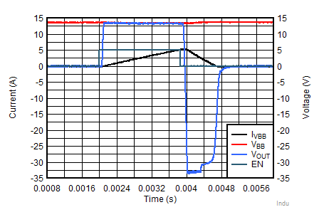
GUID-256673F3-C2B3-4DFD-934A-3EDA02656E66-low.gifFigure 9-2 Inductive Discharge (5 mH, 5 A)

In addition, the TPS27SA08-Q1 device current limit provides an ideal way to charge a capacitive load safely with limited inrush current. With no protection, charging a large capacitive load can lead to high inrush currents that pull a supply down, however by using a relatively low current limit value (regulation around 24 A), the capacitive load can be charged without impact to the power supply.

For more information on driving inductive or capacitive loads, reference TI's "How To Drive Inductive, Capacitive, and Lighting Loads with Smart High Side Switch application report.