ZHCSMM0 December   2020 TPS27SA08-Q1

PRODUCTION DATA  

  1. 特性
  2. 应用
  3. 说明
  4. Revision History
  5. Device Summary Table
  6. Pin Configuration and Functions
    1. 6.1 Recommended Connections for Unused Pins
  7. Specifications
    1. 7.1 Absolute Maximum Ratings
    2. 7.2 ESD Ratings
    3. 7.3 Recommended Operating Conditions
    4. 7.4 Thermal Information
    5. 7.5 Electrical Characteristics
    6. 7.6 Switching Characteristics
    7. 7.7 SNS Timing Characteristics
    8. 7.8 Typical Characteristics
  8. Parameter Measurement Information
  9. Detailed Description
    1. 9.1 Overview
    2. 9.2 Functional Block Diagram
    3. 9.3 Feature Description
      1. 9.3.1 Protection Mechanisms
        1. 9.3.1.1 Thermal Shutdown
        2. 9.3.1.2 Current Limit
          1. 9.3.1.2.1 Current Limit Foldback
          2. 9.3.1.2.2 Undervoltage Lockout (UVLO)
          3. 9.3.1.2.3 VBB during Short-to-Ground
        3. 9.3.1.3 Energy Limit
        4. 9.3.1.4 Voltage Transients
          1. 9.3.1.4.1 Driving Inductive and Capacitive Loads
        5. 9.3.1.5 Reverse supply
        6. 9.3.1.6 Fault Event – Timing Diagrams
      2. 9.3.2 Diagnostic Mechanisms
        1. 9.3.2.1 VOUT Short-to-supply and Open-Load
          1. 9.3.2.1.1 Detection With Switch Enabled
          2. 9.3.2.1.2 Detection With Switch Disabled
        2. 9.3.2.2 SNS Output
          1. 9.3.2.2.1 RSNS Value
            1. 9.3.2.2.1.1 High Accuracy Load Current Sense
            2. 9.3.2.2.1.2 SNS Output Filter
        3. 9.3.2.3 ST Pin
        4. 9.3.2.4 Fault Indication and SNS Mux
        5. 9.3.2.5 Resistor Sharing
        6. 9.3.2.6 High-Frequency, Low Duty-Cycle Current Sensing
    4. 9.4 Device Functional Modes
      1. 9.4.1 Off
      2. 9.4.2 Standby
      3. 9.4.3 Diagnostic
      4. 9.4.4 Standby Delay
      5. 9.4.5 Active
      6. 9.4.6 Fault
  10. 10Application and Implementation
    1. 10.1 Application Information
      1. 10.1.1 Ground Protection Network
      2. 10.1.2 Interface With Microcontroller
      3. 10.1.3 I/O Protection
      4. 10.1.4 Inverse Current
      5. 10.1.5 Loss of GND
      6. 10.1.6 Thermal Information
    2. 10.2 Typical Application
      1. 10.2.1 Design Requirements
      2. 10.2.2 Detailed Design Procedure
        1. 10.2.2.1 Thermal Considerations
        2. 10.2.2.2 Diagnostics
          1. 10.2.2.2.1 Selecting the RISNS Value
      3. 10.2.3 Application Curves
  11. 11Power Supply Recommendations
  12. 12Layout
    1. 12.1 Layout Guidelines
    2. 12.2 Layout Example
  13. 13Device and Documentation Support
    1. 13.1 Device Support
      1. 13.1.1 Related Documentation
    2. 13.2 Trademarks
    3. 13.3 Electrostatic Discharge Caution
    4. 13.4 Glossary
  14. 14Mechanical, Packaging, and Orderable Information

封装选项

机械数据 (封装 | 引脚)
散热焊盘机械数据 (封装 | 引脚)
订购信息

Fault Event – Timing Diagrams

Note:

All timing diagrams assume that the SELx pins are set to 00.

The LATCH, DIA_EN, and EN pins are controlled by the user. The timing diagrams represent a possible use-case.

Figure 9-4 shows the active current limiting behavior of TPS27SA08-Q1 device and the LATCH pin functionality. The switch will not shutdown until either the energy limit or the thermal shutdown is reached.
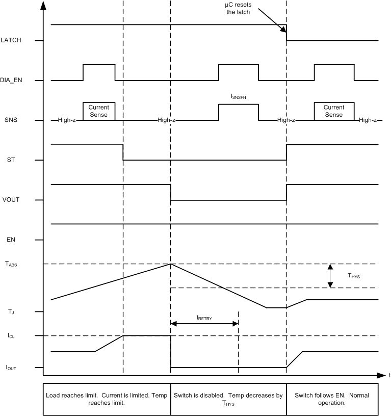
GUID-09C8A827-2777-479A-860B-ADA8F9BFAABB-low.gifFigure 9-4 Current Limit - Latched Behavior

Figure 9-5 shows the active current limiting behavior of TPS27SA08-Q1 device. The switch will not shutdown until either thermal shutdown or energy limit is tripped. In this example, LATCH is tied to GND and the switch is turned ON when the FET temperature is low enough.
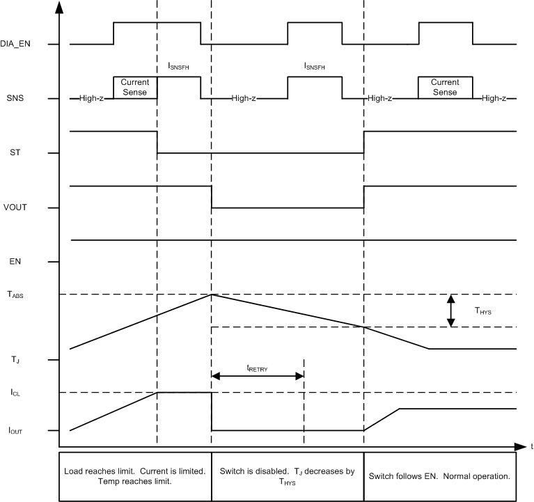
GUID-79A1B9CB-9519-4159-A5CB-BD179D8510D9-low.gifFigure 9-5 Current Limit - LATCH Pin Permanently Low

deWhen the switch retries after a shutdown event, the SNS fault indication will remain until VOUT has risen to VBB – 1.8 V. Once VOUT has risen, the SNS fault indication is reset and current sensing is available. ST fault indication is reset as soon as the switch is re-enabled (does not wait for VOUT to rise). If there is a short-to-ground and VOUT is not able to rise, the SNS fault indication will remain indefinitely. The following diagram illustrates auto-retry behavior and provides a zoomed-in view of the fault indication during retry.

Note:

Figure 9-6 assumes that tRETRY has expired by the time that TJ reaches the hysteresis threshold.

LATCH = 0 V and DIA_EN = 5 V
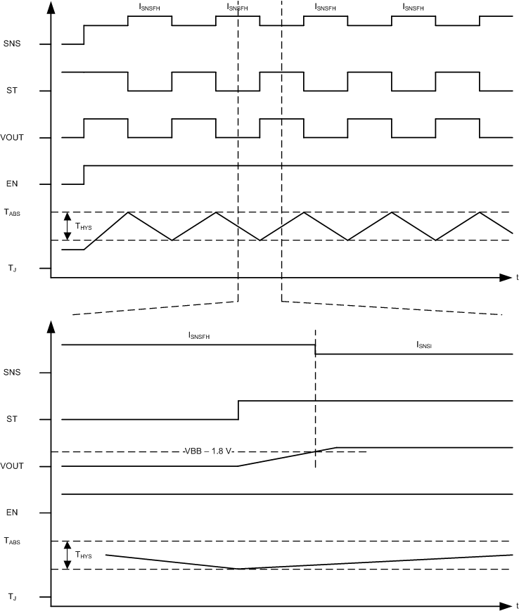
GUID-A5AC1E03-A145-4141-B1B4-749BCE615B89-low.gifFigure 9-6 Fault Indication During Retry