ZHCSET0D December   2015  – December 2019 TPS2H000-Q1

PRODUCTION DATA.  

  1. 特性
  2. 应用
  3. 说明
    1.     Device Images
      1.      典型应用原理图
      2.      驱动具有可调节电流限制的电容性负载
  4. 修订历史记录
  5. Device Comparison Table
  6. Pin Configuration and Functions
    1.     Pin Functions
  7. Specifications
    1. 7.1 Absolute Maximum Ratings
    2. 7.2 ESD Ratings
    3. 7.3 Recommended Operating Conditions
    4. 7.4 Thermal Information
    5. 7.5 Electrical Characteristics
    6. 7.6 Switching Characteristics
    7. 7.7 Typical Characteristics
  8. Detailed Description
    1. 8.1 Overview
    2. 8.2 Functional Block Diagram
    3. 8.3 Feature Description
      1. 8.3.1 Pin Current and Voltage Conventions
      2. 8.3.2 Accurate Current Sense
      3. 8.3.3 Adjustable Current Limit
      4. 8.3.4 Inductive-Load Switching-Off Clamp
      5. 8.3.5 Fault Detection and Reporting
        1. 8.3.5.1 Diagnostic Enable Function
        2. 8.3.5.2 Multiplexing of Current Sense
        3. 8.3.5.3 Fault Table
        4. 8.3.5.4 STx and FAULT Reporting
      6. 8.3.6 Full Diagnostics
        1. 8.3.6.1 Short-to-GND and Overload Detection
        2. 8.3.6.2 Open-Load Detection
          1. 8.3.6.2.1 Channel On
          2. 8.3.6.2.2 Channel Off
        3. 8.3.6.3 Short-to-Battery Detection
        4. 8.3.6.4 Reverse Polarity Detection
        5. 8.3.6.5 Thermal Fault Detection
          1. 8.3.6.5.1 Thermal Shutdown
      7. 8.3.7 Full Protections
        1. 8.3.7.1 UVLO Protection
        2. 8.3.7.2 Loss-of-GND Protection
        3. 8.3.7.3 Protection for Loss of Power Supply
        4. 8.3.7.4 Reverse-Current Protection
        5. 8.3.7.5 MCU I/O Protection
    4. 8.4 Device Functional Modes
      1. 8.4.1 Working Modes
  9. Application and Implementation
    1. 9.1 Application Information
    2. 9.2 Typical Application
      1. 9.2.1 Design Requirements
      2. 9.2.2 Detailed Design Procedure
      3. 9.2.3 Application Curves
  10. 10Power Supply Recommendations
  11. 11Layout
    1. 11.1 Layout Guidelines
    2. 11.2 Layout Examples
      1. 11.2.1 Without a GND Network
      2. 11.2.2 With a GND Network
  12. 12器件和文档支持
    1. 12.1 接收文档更新通知
    2. 12.2 社区资源
    3. 12.3 商标
    4. 12.4 静电放电警告
    5. 12.5 Glossary
  13. 13机械、封装和可订购信息

封装选项

机械数据 (封装 | 引脚)
散热焊盘机械数据 (封装 | 引脚)
订购信息

Thermal Shutdown

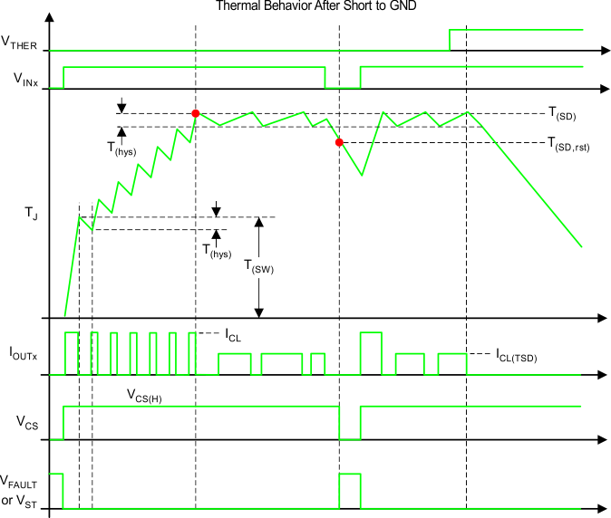
Thermal shutdown is active when the absolute temperature TJ > T(SD). When thermal shutdown occurs, the respective output turns off. The THER pin is used to configure the behavior after the thermal shutdown occurs.

  • When the THER pin is low, thermal shutdown operates in the auto-retry mode. The output automatically recovers when TJ < T(SD) – T(hys), but the current is limited to ICL(TSD) to avoid repetitive thermal shutdown. The thermal shutdown fault signal is cleared when TJ < T(SD,rst) or after toggling the related INx pin.
  • When the THER pin is high, thermal shutdown operates in the latch mode. The output latches off when thermal shutdown occurs. When the THER pin goes from high to low, thermal shutdown changes to auto-retry mode. The thermal shutdown fault signal is cleared after toggling the related INx pin.

Thermal swing activates when the power FET temperature is increasing sharply, that is, when ΔT = T(FET) – T(Logic) > T(sw), then the output turns off. The output automatically recovers and the fault signal clears when ΔT = T(FET) – T(Logic) < T(sw) – T(hys). Thermal swing function improves the device reliability when subjected to repetitive fast thermal variation. As shown in Figure 33, multiple thermal swings are triggered before thermal shutdown occurs.
TPS2H000-Q1 therm-dgm_SLVSCV8.gifFigure 33. Thermal Behavior Diagram