ZHCSET0D December 2015 – December 2019 TPS2H000-Q1
PRODUCTION DATA.
- 1 特性
- 2 应用
- 3 说明
- 4 修订历史记录
- 5 Device Comparison Table
- 6 Pin Configuration and Functions
- 7 Specifications
-
8 Detailed Description
- 8.1 Overview
- 8.2 Functional Block Diagram
- 8.3 Feature Description
- 8.4 Device Functional Modes
- 9 Application and Implementation
- 10Power Supply Recommendations
- 11Layout
- 12器件和文档支持
- 13机械、封装和可订购信息
8.3.7.4 Reverse-Current Protection
Reverse current occurs in two conditions: short to battery and reverse polarity.
- When a short to the battery occurs, there is only reverse current through the body diode. IR(1) specifies the limit of the reverse current.
- In a reverse-polarity condition, there are reverse currents through the body diode and the device GND pin. IR(2) specifies the limit of the reverse current. The GND pin maximum current is specified in the Absolute Maximum Ratings.
To protect the device, TI recommends two types of external circuitry.
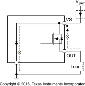
- Adding a blocking diode. Both the IC and load are protected when in reverse polarity.
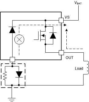
- Adding a GND network. The reverse current through the device GND is blocked. The reverse current through the FET is limited by the load itself. TI recommends a resistor in parallel with the diode as a GND network. The recommended selection are 1-kΩ resistor in parallel with an >100-mA diode. If multiple high-side switches are used, the resistor and diode can be shared among devices. The reverse current protection diode in the GND network forward voltage should be less than 0.6 V in any circumstances. In addition a minimum resistance of 4.7 K is recommended on the I/O pins.
 Figure 35. Reverse-Current External Protection, Method 1
  Figure 36. Reverse-Current External Protection, Method 2