ZHCSAS6B August   2012  – April 2015

PRODUCTION DATA.  

  1. 特性
  2. 应用范围
  3. 说明
  4. 修订历史记录
  5. Pin Configuration and Functions
  6. Specifications
    1. 6.1 Absolute Maximum Ratings
    2. 6.2 ESD Ratings
    3. 6.3 Recommended Operating Conditions
    4. 6.4 Thermal Information
    5. 6.5 Electrical Characteristics
    6. 6.6 Timing Requirements
    7. 6.7 Typical Characteristics
  7. Detailed Description
    1. 7.1 Overview
    2. 7.2 Functional Block Diagrams
    3. 7.3 Feature Description
      1. 7.3.1 Push-Button Timer Selection (TS)
      2. 7.3.2 Inputs
        1. 7.3.2.1 TPS3420 Inputs (PB1, PB2)
        2. 7.3.2.2 TPS3421 Inputs (PB1, PB2)
        3. 7.3.2.3 TPS3422 Inputs (PB1)
      3. 7.3.3 Output (RST)
    4. 7.4 Device Functional Modes
      1. 7.4.1 Normal Operation (VDD > 1.6 V)
      2. 7.4.2 Below VDD(min) (1.6 V > VDD > 1.3 V)
      3. 7.4.3 Power-On Reset (VDD < 1.3 V)
  8. Application and Implementation
    1. 8.1 Application Information
    2. 8.2 Typical Applications
      1. 8.2.1 Single Input With Fixed Reset Pulse Duration
        1. 8.2.1.1 Design Requirements
        2. 8.2.1.2 Detailed Design Procedure
        3. 8.2.1.3 Application Curve
      2. 8.2.2 Dual Input Applications
        1. 8.2.2.1 Design Requirements
        2. 8.2.2.2 Detailed Design Procedure
        3. 8.2.2.3 Application Curve
      3. 8.2.3 Latched Reset Signal
        1. 8.2.3.1 Design Requirements
        2. 8.2.3.2 Detailed Design Procedure
        3. 8.2.3.3 Application Curve
  9. Power Supply Recommendations
  10. 10Layout
    1. 10.1 Layout Guidelines
    2. 10.2 Layout Example
  11. 11器件和文档支持
    1. 11.1 器件支持
      1. 11.1.1 开发支持
        1. 11.1.1.1 评估模块
        2. 11.1.1.2 Spice 模型
      2. 11.1.2 器件命名规则
    2. 11.2 文档支持
      1. 11.2.1 相关文档
    3. 11.3 相关链接
    4. 11.4 商标
    5. 11.5 静电放电警告
    6. 11.6 术语表
  12. 12机械封装和可订购信息

封装选项

机械数据 (封装 | 引脚)
散热焊盘机械数据 (封装 | 引脚)
订购信息

10 Layout

10.1 Layout Guidelines

Follow these guidelines for laying out the printed circuit board (PCB) that is used for the TPS342x.

  • Place the VCC decoupling capacitor close to the device.
  • Avoid using long traces for the VCC supply node. The VDD capacitor (CVDD), along with parasitic inductance from the supply to the capacitor, can form an LC tank and create ringing with peak voltages above the maximum VCC voltage.

10.2 Layout Example
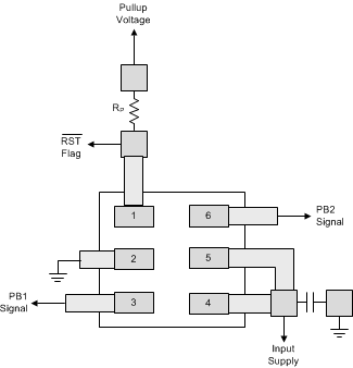
TPS342 LayoutDRY_sbvs211.gifFigure 21. Layout Example (DRY Package)