ZHCSAS6B August 2012 – April 2015
PRODUCTION DATA.
- 1 特性
- 2 应用范围
- 3 说明
- 4 修订历史记录
- 5 Pin Configuration and Functions
- 6 Specifications
- 7 Detailed Description
- 8 Application and Implementation
- 9 Power Supply Recommendations
- 10Layout
- 11器件和文档支持
- 12机械封装和可订购信息
5 Pin Configuration and Functions
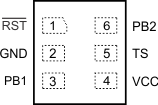
TPS3420, TPS3421: DRY Package
6-Pin USON
Top View

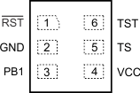
TPS3422: DRY Package
6-Pin USON
Top View

Pin Functions
| PIN | I/O | DESCRIPTION | ||
|---|---|---|---|---|
| NAME | TPS3420/21 | TPS3422 | ||
| GND | 2 | 2 | — | Ground. |
| PB1 | 3 | 3 | I | Push-button input. PB1 and PB2 must be held low for greater than tTIMER time to assert the reset output. |
| PB2 | 6 | — | I | Second push-button input. PB1 and PB2 must be held low for greater than tTIMER time to assert the reset output. |
| RST | 1 | 1 | O | Active low, open-drain output. Reset is asserted (goes low) when both PB1 and PB2 are held low for longer than tTIMER time (only PB1 for TPS3422). For TPS3420: Reset is deasserted when either PBx input goes high. For TPS3421,TPS3422: Reset is deasserted after fixed time of tRST. |
| TS | 5 | 5 | I | Time delay selection input. Connect to VCC or GND for different tTIMER selections. In normal operation, the TS pin state should not be changed because it is intended to be permanently connected to either GND or VCC. If switching the TS pin is required, it should be done during power off, or when either PBx input is high. |
| TST | — | 6 | — | Connect this pin to GND or VCC during normal device operation. |
| VCC | 4 | 4 | I | Supply voltage input. Connect a 1.6-V to 6.5-V supply to VCC to power the device. It is good analog design practice to place a 0.1-µF ceramic capacitor close to this pin. |