ZHCSAS6B August 2012 – April 2015
PRODUCTION DATA.
- 1 特性
- 2 应用范围
- 3 说明
- 4 修订历史记录
- 5 Pin Configuration and Functions
- 6 Specifications
- 7 Detailed Description
- 8 Application and Implementation
- 9 Power Supply Recommendations
- 10Layout
- 11器件和文档支持
- 12机械封装和可订购信息
7 Detailed Description
7.1 Overview
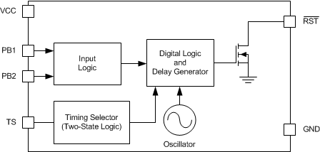
The TPS342x are a family of push-button reset devices with an extended setup period that prevents resets from occurring as a result of short-duration switch closures. See Table 1 for details.
The TPS3420 is a dual-channel device with an output that asserts when both inputs (PB1 and PB2) are held low for the push-button timer duration, and deasserts when either input PBx is released.
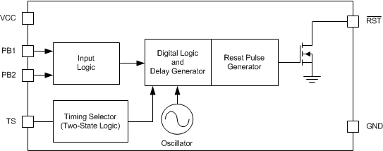
The TPS3421 is a dual-channel device with an output that asserts when both inputs (PB1 and PB2) are held low for the push-button timer duration, and deasserts after the reset time-out duration.
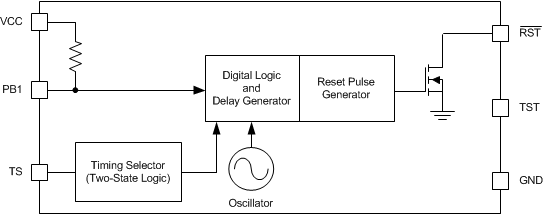
The TPS3422 is a single-channel device with an output that asserts when the PB1 input is held low for the push-button timer duration, and deasserts after the reset time-out duration.
The TPS342x family also has a TS pin that selects between two different push-button timing options by connecting the pin to either GND or VCC.
Table 1. Device Family Options
| DEVICE | CHANNELS | INPUT | RESET BEHAVIOR (DEASSERTION) |
|---|---|---|---|
| TPS3420 | 2 | NMOS-based threshold | Input (PBx) dependent |
| TPS3421 | 2 | External pullup to VCC | Fixed pulse |
| TPS3422 | 1 | Internal pullup | Fixed pulse |
7.2 Functional Block Diagrams


7.3 Feature Description
7.3.1 Push-Button Timer Selection (TS)
The TPS342x offer two different push-button timer options (tTIMER) for system flexibility with the use of the TS pin. Connect the TS pin to either GND or VCC for two different timing options, as shown in Table 2.
Table 2. Push-Button Timer Option Examples
| PRODUCT | PUSH-BUTTON TIMER | RESET PULSE | |
|---|---|---|---|
| TS = VCC | TS = GND | ||
| TPS3420DDRYR/T | 12.5 s | 7.5 s | N/A |
| TPS3421EGDRYR/T | 0 s | 7.5 s | 400 ms |
| TPS3422EGDRYR/T | 0 s | 7.5 s | 400 ms |
During normal operation, the TS pin state should not be changed because TS is intended to be permanently connected to either ground or VCC. The state of the TS pin is checked during power up and when either PBx input is high. Therefore, if a different timing option is desired, the state must be changed during power off, or when either PBx input is high, to avoid false operation.
7.3.2 Inputs
This section discusses the inputs of the TPS342x devices.
7.3.2.1 TPS3420 Inputs (PB1, PB2)
The TPS3420 has two NMOS-based threshold inputs (PB1, PB2) with a VIH ≥ 0.85 V, and a VIL ≤ 0.3 V. When input conditions are met (that is, when both inputs are simultaneously held low for the push-button timer period, tTIMER), the device asserts a reset low, as shown in Figure 1. Reset deassertion occurs when either input goes high. The reset pulse occurs only one time after each valid input condition. At least one input pin must be released (goes high) and then driven low for the tTIMER period before RST asserts again.
7.3.2.2 TPS3421 Inputs (PB1, PB2)
The TPS3421 has two inputs: PB1 and PB2. External pullup resistors to VCC are required to pull the input pins high. When input conditions are met (that is, when both inputs are held low simultaneously for the push-button timer period, tTIMER), the device asserts a single reset pulse of a fixed time (tRST); see Figure 2. Reset deassertion is independent of the inputs because tRST is a fixed time pulse. A reset pulse occurs only one time after each valid input condition. At least one input pin must be released (go high) and then driven low for the tTIMER duration before RST asserts again.
7.3.2.3 TPS3422 Inputs (PB1)
The TPS3422 has only one input: PB1. This input has an internal pullup resistor to VCC. When input conditions are met (that is, when the input is held low for the push-button timer period, tTIMER), the device asserts a single reset pulse of a fixed time (tRST); see Figure 3. Reset deassertion is independent of the input because tRST is a fixed time pulse. A reset pulse occurs only one time after each valid input condition. The input pin must be released (go high) and then driven low for the tTIMER period before RST asserts again.
7.3.3 Output (RST)
The TPS342x have an open-drain output. A pullup resistor must be used to hold the line high when the output is in a high-impedance state (not asserted). By connecting a pullup resistor to the proper voltage rail, the output can be connected to other devices at correct interface voltage levels. The TPS342x output can be pulled up to 6.5 V, independent of the device supply voltage. To ensure proper voltage levels, make sure to choose the correct pullup resistor values. The pullup resistor value is determined by VOL, sink current capability, and output leakage current (Ilkg(OD)). These values are specified in Electrical Charactersitcs.
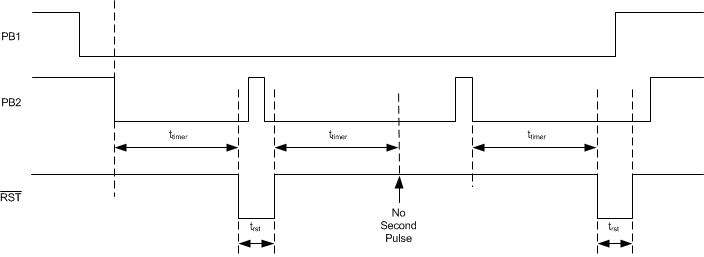
The Inputs (PB1, PB2) describes how the output is asserted or deasserted. See Figure 1 (TPS3420), Figure 2 (TPS3421), or Figure 3 (TPS3422) for a timing diagram that describes the relationship between the PB1 and PB2 inputs and the output. Figure 14 shows the TPS3421 reset timing.
 Figure 14. TPS3421 Reset Timing Diagram
Any change in input condition is detected after reset is deasserted. If input PB1 or PB2 has a pulse (low-to-high-to-low) during the tRST period, the change is not recognized by the device. If input PB1 or PB2 go high during the tRST period, the change is detected after reset is deasserted.
7.4 Device Functional Modes
7.4.1 Normal Operation (VDD > 1.6 V)
When the voltage on VDD is greater than 1.6 V (VDD(min)) for approximately 300 μs (tSD), the RST signal corresponds to the state of the PB1 and PB2 pins; see Table 1.
7.4.2 Below VDD(min) (1.6 V > VDD > 1.3 V)
When the voltage on VDD is less than 1.6 V but greater than 1.3 V (typical), the RST signal corresponds to the state of the PB1 and PB2 pins; however, the electrical specifications in the Electrical Characteristics and Timing Requirements tables do not apply when VDD < VDD(min).
7.4.3 Power-On Reset (VDD < 1.3 V)
When the voltage on VDD is lower than 1.3 V (typical), the RST output should be high-impedance. However, it is not ensured to be in a high impedance state under all conditions.