ZHCSIK1A July 2018 – September 2021 TPS3430-Q1
PRODUCTION DATA
- 1 特性
- 2 应用
- 3 说明
- 4 Revision History
- 5 Pin Configuration and Functions
- 6 Specifications
- 7 Detailed Description
- 8 Application and Implementation
- 9 Power Supply Recommendations
- 10Layout
- 11Device and Documentation Support
- 12Mechanical, Packaging, and Orderable Information
5 Pin Configuration and Functions
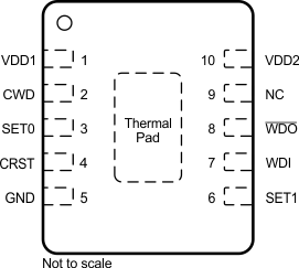
 Figure 5-1 DRC
Package
Figure 5-1 DRC
Package3-mm × 3-mm VSON-10
Top View
Table 5-1 Pin Functions
| PIN | I/O | DESCRIPTION | |
|---|---|---|---|
| NAME | NO. | ||
| VDD1 | 1 | I | Supply voltage pin. For noisy systems, connecting a 0.1-µF bypass capacitor is recommended. |
| CWD | 2 | I | Programmable watchdog timeout
input. Watchdog timeout is set by connecting a capacitor between
this pin and ground. Furthermore, this pin can also be connected by
a 10-kΩ resistor to VDD, or leaving unconnected (NC) further enables
the selection of the preset watchdog timeouts; see the Section 6.6 table. When using a capacitor, the TPS3430-Q1 determines the window watchdog upper boundary with Equation 4. The lower watchdog boundary is set by the SET pins, see Table 8-7 and the Section 8.1.2 section for additional information. |
| SET0 | 3 | I | Logic input. SET0, SET1, and CWD select the watchdog window ratios, timeouts, and disable the watchdog; see the Section 6.6 table. |
| CRST | 4 | I | Programmable watchdog reset
delay pin. Connect a capacitor between this pin and GND to program
the watchdog reset delay period. This pin can also be connected by a
10-kΩ pull-up resistor to VDD, or left unconnected (NC) for various
factory programmed watchdog reset delay options; see the Section 8.1.1 section. When using an external capacitor, use Equation 1 to determine the watchdog reset delay. |
| GND | 5 | — | Ground pin |
| SET1 | 6 | I | Logic input. SET0, SET1, and CWD select the watchdog window ratios, timeouts, and disable the watchdog; see the Section 6.6 table. |
| WDI | 7 | I | Watchdog input. A falling
transition (edge) must occur at this pin within the watchdog timeout
between the lower (tWDL(max)) and upper
(tWDU(min)) window boundaries in order for
WDO to not assert. During power up, all
pulses to WDI are ignored before tRST expires and the
watchdog is disabled. When the watchdog is not in use, the SET pins can be used to disable the watchdog. The input at WDI is ignored when WDO is low (asserted) and also when the watchdog is disabled. If the watchdog is disabled, then WDI cannot be left unconnected and must be driven to either VDD or GND. |
| WDO | 8 | O | Watchdog open-drain active-low output. Connect WDO with a 1-kΩ to 100-kΩ resistor to VDD or another power supply. WDO goes low (asserts) when a watchdog timeout occurs. When a watchdog timeout occurs, WDO goes low (asserts) for the set WDO reset delay (tRST). When the watchdog is disabled, WDO remains logic high regardless of WDI. |
| NC | 9 | NC | This pin is no-connect and should be left floating. |
| VDD2 | 10 | I | Connect this pin to VDD1. The device will not function properly if VDD1 and VDD2 are not externally connected. |
| Thermal pad | — | Connect the thermal pad to a large-area ground plane. The thermal pad is internally connected to GND. | |