ZHCSIK1A July   2018  – September 2021 TPS3430-Q1

PRODUCTION DATA  

  1. 特性
  2. 应用
  3. 说明
  4. Revision History
  5. Pin Configuration and Functions
    1.     Pin Functions
  6. Specifications
    1. 6.1 Absolute Maximum Ratings
    2. 6.2 ESD Ratings
    3. 6.3 Recommended Operating Conditions
    4. 6.4 Thermal Information
    5. 6.5 Electrical Characteristics
    6. 6.6 Timing Requirements
    7. 6.7 Timing Diagrams
    8. 6.8 Typical Characteristics
  7. Detailed Description
    1. 7.1 Overview
    2. 7.2 Functional Block Diagrams
    3. 7.3 Feature Description
      1. 7.3.1 CRST
      2. 7.3.2 Window Watchdog
        1. 7.3.2.1 SET0 and SET1
          1. 7.3.2.1.1 Enabling the Window Watchdog
          2. 7.3.2.1.2 Disabling the Watchdog Timer When Using the CRST Capacitor
          3. 7.3.2.1.3 SET0 and SET1 During Normal Watchdog Operation
      3. 7.3.3 Window Watchdog Timer
        1. 7.3.3.1 CWD
        2. 7.3.3.2 WDI Functionality
        3. 7.3.3.3 WDO Functionality
    4. 7.4 Device Functional Modes
      1. 7.4.1 VDD is Below VPOR ( VDD < VPOR)
      2. 7.4.2 VDD is Above VPOR And Below VDD (min)( VPOR < VDD < VDD (min))
      3. 7.4.3 Normal Operation (VDD ≥ VDD (min))
  8. Application and Implementation
    1. 8.1 Application Information
      1. 8.1.1 CRST Delay
        1. 8.1.1.1 Factory-Programmed Watchdog Reset Delay Timing
        2. 8.1.1.2 CRST Programmable Watchdog Reset Delay
      2. 8.1.2 CWD Functionality
        1. 8.1.2.1 Factory-Programmed Timing Options
        2. 8.1.2.2 CWD Adjustable Capacitor Watchdog Timeout
        3. 8.1.2.3 42
    2. 8.2 Typical Applications
      1. 8.2.1 Monitoring Microcontroller with Watchdog Timer - Design 1
        1. 8.2.1.1 Design Requirements - Design 1
        2. 8.2.1.2 Detailed Design Procedure - Design 1
          1. 8.2.1.2.1 Meeting the Minimum Watchdog Reset Delay - Design 1
          2. 8.2.1.2.2 Setting the Watchdog Window - Design 1
          3. 8.2.1.2.3 Calculating the WDO Pull-up Resistor - Design 1
      2. 8.2.2 Monitoring Microcontroller with a Programmed Window Watchdog Timer - Design 2
        1. 8.2.2.1 Design Requirements - Design 2
        2. 8.2.2.2 Detailed Design Procedure - Design 2
          1. 8.2.2.2.1 Meeting the Minimum Watchdog Reset Delay - Design 2
          2. 8.2.2.2.2 Setting the Watchdog Window - Design 2
          3. 8.2.2.2.3 Calculating the WDO Pull-up Resistor - Design 2
      3. 8.2.3 Monitoring Microcontroller with a Latching Window Watchdog Timer - Design 3
        1. 8.2.3.1 Design Requirements - Design 3
        2. 8.2.3.2 Detailed Design Procedure - Design 3
          1. 8.2.3.2.1 Meeting the Latching Output Requirement - Design 3
          2. 8.2.3.2.2 Setting the Watchdog Window - Design 3
        3. 8.2.3.3 Application Curve - Design 3
  9. Power Supply Recommendations
  10. 10Layout
    1. 10.1 Layout Guidelines
    2. 10.2 Layout Example
  11. 11Device and Documentation Support
    1. 11.1 Device Support
    2. 11.2 Documentation Support
      1. 11.2.1 Related Documentation
    3. 11.3 接收文档更新通知
    4. 11.4 支持资源
    5. 11.5 Trademarks
    6. 11.6 Electrostatic Discharge Caution
    7. 11.7 术语表
  12. 12Mechanical, Packaging, and Orderable Information

封装选项

机械数据 (封装 | 引脚)
散热焊盘机械数据 (封装 | 引脚)
订购信息
SET0 and SET1 During Normal Watchdog Operation

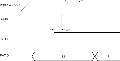
The SET0 and SET1 pins can be used to control the window watchdog ratio of the lower boundary to the upper boundary. There are four possible modes for the watchdog (see Table 8-7): disabled, 1:8 ratio, 3:4 ratio, and 1:2 ratio. If SET0 = 1 and SET1 = 0, then the watchdog is disabled. When the watchdog is disabled WDO does not assert, and the TPS3430-Q1 ignores all inputs to WDI. The SET0 and SET1 pins can be changed when the device is operational, but cannot be changed at the same time. If these pins are changed when the device is operational, then there must be a 500-µs (tSET) delay between switching the two pins. If the SET0 and SET1 are used to change the reset timing, then a reset event must occur before the new timing condition is latched. This reset can be triggered by bringing VDD below VUVLO. Figure 7-4 shows how the SET0 and SET1 pins do not change the watchdog timing option until a reset event has occurred.
GUID-768050BA-559C-4E9C-91A8-A93D976A1A7B-low.gifFigure 7-4 Changing SET0 and SET1 Pins