ZHCSCB4C march 2014 – march 2021 TPS3700-Q1
PRODUCTION DATA
- 1 特性
- 2 应用
- 3 说明
- 4 Revision History
- 5 Pin Configuration and Functions
- 6 Specifications
- 7 Detailed Description
- 8 Application and Implementation
- 9 Power Supply Recommendations
- 10Layout
- 11Device and Documentation Support
- 12Mechanical, Packaging, and Orderable Information
5 Pin Configuration and Functions
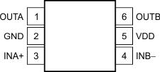
 Figure 5-1 DDC Package
 SOT-6
Top View
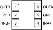
 Figure 5-2 DSE Package
WSON-6
Top View
Table 5-1 Pin Functions
| PIN | I/O | DESCRIPTION | ||
|---|---|---|---|---|
| NAME | DDC | DSE | ||
| GND | 2 | 5 | — | Ground |
| INA+ | 3 | 4 | I | This pin is connected to the voltage to be monitored with the use of an external resistor divider. When the voltage at this terminal drops below the threshold voltage (VIT+ – VHYS), OUTA is driven low. |
| INB– | 4 | 3 | I | This pin is connected to the voltage to be monitored with the use of an external resistor divider. When the voltage at this terminal exceeds the threshold voltage (VIT+), OUTB is driven low. |
| OUTA | 1 | 6 | O | INA+ comparator open-drain output. OUTA is driven low when the voltage at this comparator is below (VIT+ – VHYS). The output goes high when the sense voltage returns above the respective threshold (VIT+). |
| OUTB | 6 | 1 | O | INB– comparator open-drain output. OUTB is driven low when the voltage at this comparator exceeds VIT+. The output goes high when the sense voltage returns below the respective threshold (VIT+ – VHYS). |
| VDD | 5 | 2 | I | Supply voltage input. Connect a 1.8-V to 18-V supply to VDD to power the device. Good analog design practice is to place a 0.1-µF ceramic capacitor close to this pin. |