ZHCSDQ6C April   2015  – March 2024 TPS3702-Q1

PRODUCTION DATA  

  1.   1
  2. 特性
  3. 应用
  4. 说明
  5. Pin Configuration and Functions
  6. Specifications
    1. 5.1 Absolute Maximum Ratings
    2. 5.2 ESD Ratings
    3. 5.3 Recommended Operating Conditions
    4. 5.4 Thermal Information
    5. 5.5 Electrical Characteristics
    6. 5.6 Timing Requirements
    7. 5.7 Typical Characteristics
  7. Detailed Description
    1. 6.1 Overview
    2. 6.2 Functional Block Diagram
    3. 6.3 Feature Description
      1. 6.3.1 Input (SENSE)
      2. 6.3.2 Outputs (UV, OV)
      3. 6.3.3 User-Configurable Accuracy Band (SET)
    4. 6.4 Device Functional Modes
      1. 6.4.1 Normal Operation (VDD > UVLO)
      2. 6.4.2 Undervoltage Lockout (V(POR) < VDD < UVLO)
      3. 6.4.3 Power-On Reset (VDD < V(POR))
  8. Application and Implementation
    1. 7.1 Application Information
      1. 7.1.1 Window Voltage Detector Considerations
      2. 7.1.2 Input and Output Configurations
      3. 7.1.3 Immunity to SENSE Pin Voltage Transients
    2. 7.2 Typical Application
      1. 7.2.1 Design Requirements
      2. 7.2.2 Detailed Design Procedure
      3. 7.2.3 Application Curves
    3. 7.3 Power Supply Recommendations
    4. 7.4 Layout
      1. 7.4.1 Layout Guidelines
      2. 7.4.2 Layout Example
  9. Device and Documentation Support
    1. 8.1 Device Support
      1. 8.1.1 Development Support
        1. 8.1.1.1 Evaluation Module
      2. 8.1.2 Device Nomenclature
    2. 8.2 Documentation Support
      1. 8.2.1 Related Documentation
    3. 8.3 支持资源
    4. 8.4 Trademarks
    5. 8.5 静电放电警告
    6. 8.6 术语表
  10. Revision History
  11. 10Mechanical, Packaging, and Orderable Information

封装选项

机械数据 (封装 | 引脚)
散热焊盘机械数据 (封装 | 引脚)
订购信息

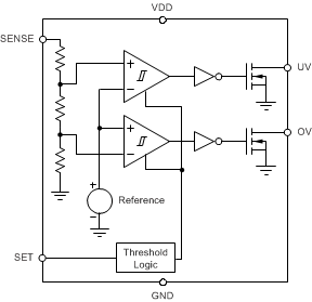
Functional Block Diagram

GUID-AF4C7F34-C404-4F81-9947-4C944BDA1587-low.gif