ZHCSIZ9D November   2018  – March 2021 TPS3703-Q1

PRODUCTION DATA  

  1. 特性
  2. 应用
  3. 说明
  4. Revision History
  5. Device Comparison
  6. Pin Configuration and Functions
  7. Specifications
    1. 7.1 Absolute Maximum Ratings
    2. 7.2 ESD Ratings
    3. 7.3 Recommended Operating Conditions
    4. 7.4 Thermal Information
    5. 7.5 Electrical Characteristics
    6. 7.6 Timing Requirements
    7. 7.7 Timing Diagrams
    8. 7.8 Typical Characteristics
  8. Detailed Description
    1. 8.1 Overview
    2. 8.2 Functional Block Diagram
    3. 8.3 Feature Description
      1. 8.3.1 VDD
      2. 8.3.2 SENSE
      3. 8.3.3 RESET
      4. 8.3.4 Capacitor Time (CT)
      5. 8.3.5 Manual Reset ( MR)
    4. 8.4 Device Functional Modes
      1. 8.4.1 Normal Operation (VDD > VDD(MIN))
      2. 8.4.2 Undervoltage Lockout (VPOR < VDD < UVLO)
      3. 8.4.3 Power-On Reset (VDD < VPOR)
  9. Application and Implementation
    1. 9.1 Application Information
      1. 9.1.1 Voltage Threshold Accuracy
      2. 9.1.2 CT Reset Time Delay
        1. 9.1.2.1 Factory-Programmed Reset Delay Timing
        2. 9.1.2.2 Programmable Reset Delay-Timing
      3. 9.1.3 RESET Latch Mode
      4. 9.1.4 Adjustable Voltage Thresholds
      5. 9.1.5 Immunity to SENSE Pin Voltage Transients
        1. 9.1.5.1 Hysteresis
    2. 9.2 Typical Applications
      1. 9.2.1 Design 1: Multi-Rail Window Monitoring for Microcontroller Power Rails
        1. 9.2.1.1 Design Requirements
        2. 9.2.1.2 Detailed Design Procedure
        3. 9.2.1.3 Application Curves
      2. 9.2.2 Design 2: RESET Latch Mode
        1. 9.2.2.1 Design Requirements
        2. 9.2.2.2 Detailed Design Procedure
        3. 9.2.2.3 Application Curves
  10. 10Power Supply Recommendations
    1. 10.1 Power Supply Guidelines
  11. 11Layout
    1. 11.1 Layout Guidelines
    2. 11.2 Layout Example
  12. 12Device and Documentation Support
    1. 12.1 Device Support
      1. 12.1.1 Device Nomenclature
    2. 12.2 Documentation Support
      1. 12.2.1 Evaluation Module
    3. 12.3 接收文档更新通知
    4. 12.4 支持资源
    5. 12.5 Trademarks
    6. 12.6 静电放电警告
    7. 12.7 术语表
  13. 13Mechanical, Packaging, and Orderable Information

封装选项

机械数据 (封装 | 引脚)
散热焊盘机械数据 (封装 | 引脚)
订购信息

Application Curves

GUID-0895A6FB-72CD-4A83-852C-08FD4B24FD77-low.gif
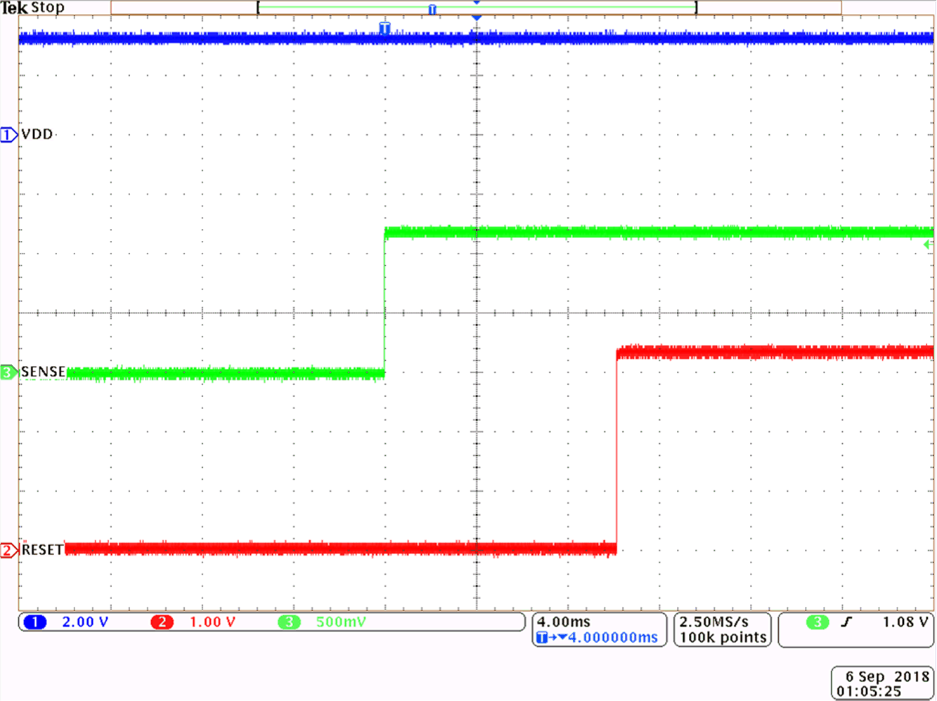
VSENSE Start up from 0 V to 1.2 V, VDD = 3.3 V, CT = OPEN VRESET = VDD = 3.3 V, TPS3703A4120
Figure 9-7 TPS3703-Q1 SENSE Start Up Function
GUID-25B78626-32C0-4203-A16D-01A7BB89B39B-low.gif
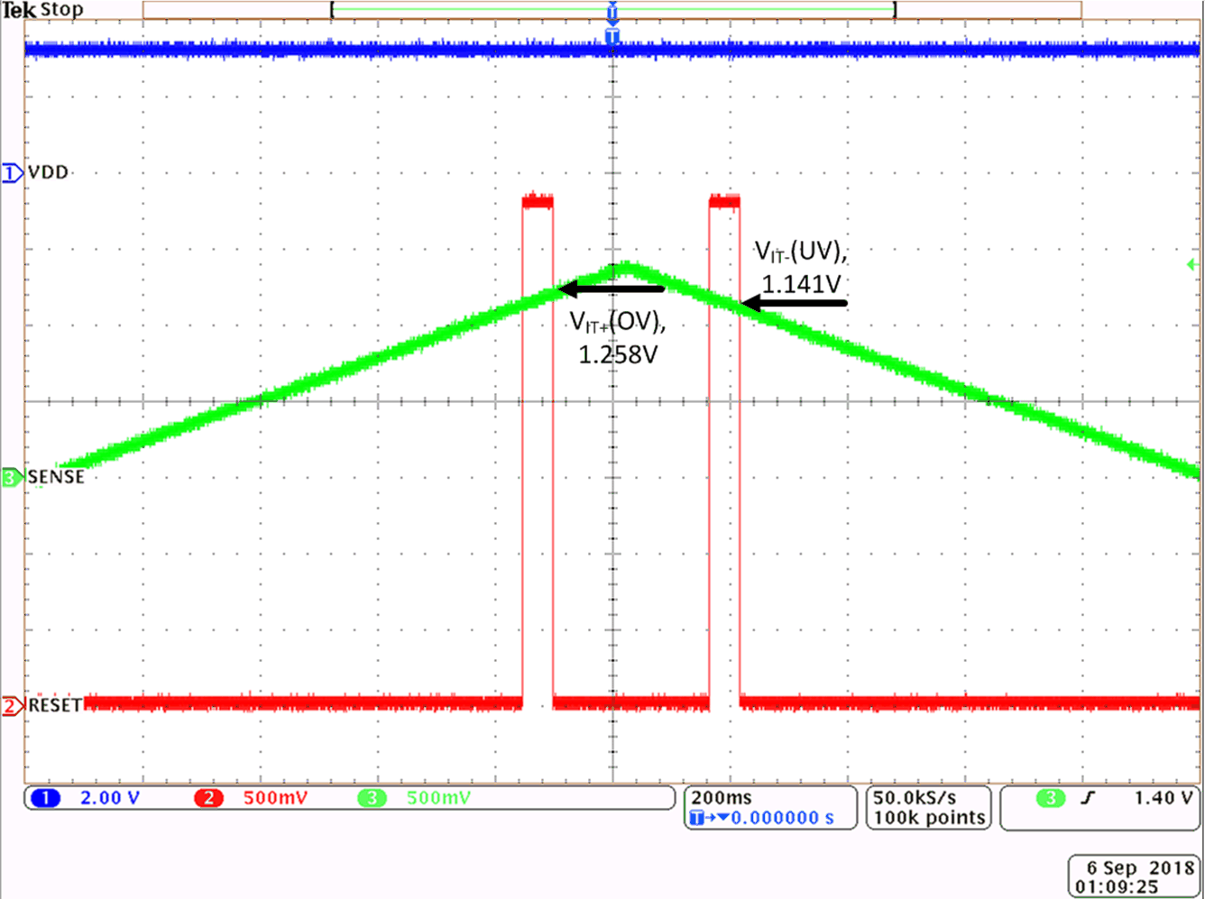
VSENSE ramp from 0 V to 1.4 V, VDD = 3.3 V, CT = OPEN VRESET = VDD = 3.3 V, TPS3703A4120
Figure 9-9 TPS3703-Q1 Overvoltage and Undervoltage Function
GUID-9D3B8B11-10BC-4A33-A264-1BF921B207C7-low.gif
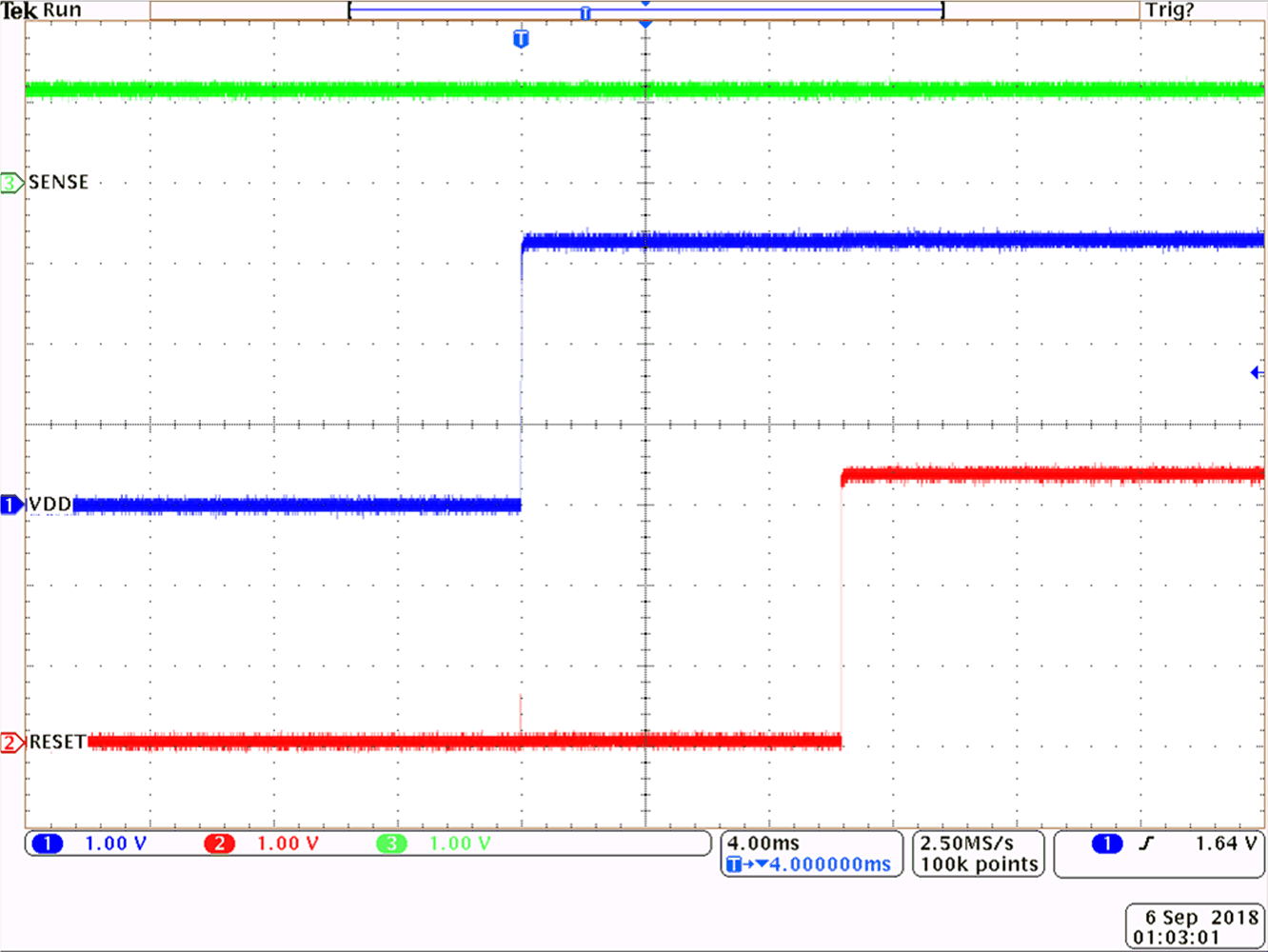
VDD Start up from 0 V to 3.3 V, VSENSE = 1.2 V, CT = OPEN VRESET = VDD = 3.3 V, TPS3703A4120
Figure 9-8 TPS3703-Q1 VDD Start Up Function
GUID-320BE7C4-469C-4646-BDAF-A400CDED7B71-low.gif
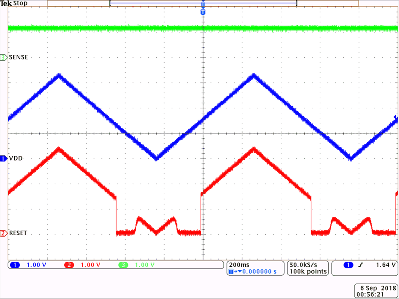
VDD ramp from 0 V to 3.3 V, VSENSE = 1.2 V, CT = OPEN VRESET = VDD = 3.3 V,TPS3703A4120
Figure 9-10 TPS3703-Q1 VDD Ramp Up Function