ZHCSIZ9D November   2018  – March 2021 TPS3703-Q1

PRODUCTION DATA  

  1. 特性
  2. 应用
  3. 说明
  4. Revision History
  5. Device Comparison
  6. Pin Configuration and Functions
  7. Specifications
    1. 7.1 Absolute Maximum Ratings
    2. 7.2 ESD Ratings
    3. 7.3 Recommended Operating Conditions
    4. 7.4 Thermal Information
    5. 7.5 Electrical Characteristics
    6. 7.6 Timing Requirements
    7. 7.7 Timing Diagrams
    8. 7.8 Typical Characteristics
  8. Detailed Description
    1. 8.1 Overview
    2. 8.2 Functional Block Diagram
    3. 8.3 Feature Description
      1. 8.3.1 VDD
      2. 8.3.2 SENSE
      3. 8.3.3 RESET
      4. 8.3.4 Capacitor Time (CT)
      5. 8.3.5 Manual Reset ( MR)
    4. 8.4 Device Functional Modes
      1. 8.4.1 Normal Operation (VDD > VDD(MIN))
      2. 8.4.2 Undervoltage Lockout (VPOR < VDD < UVLO)
      3. 8.4.3 Power-On Reset (VDD < VPOR)
  9. Application and Implementation
    1. 9.1 Application Information
      1. 9.1.1 Voltage Threshold Accuracy
      2. 9.1.2 CT Reset Time Delay
        1. 9.1.2.1 Factory-Programmed Reset Delay Timing
        2. 9.1.2.2 Programmable Reset Delay-Timing
      3. 9.1.3 RESET Latch Mode
      4. 9.1.4 Adjustable Voltage Thresholds
      5. 9.1.5 Immunity to SENSE Pin Voltage Transients
        1. 9.1.5.1 Hysteresis
    2. 9.2 Typical Applications
      1. 9.2.1 Design 1: Multi-Rail Window Monitoring for Microcontroller Power Rails
        1. 9.2.1.1 Design Requirements
        2. 9.2.1.2 Detailed Design Procedure
        3. 9.2.1.3 Application Curves
      2. 9.2.2 Design 2: RESET Latch Mode
        1. 9.2.2.1 Design Requirements
        2. 9.2.2.2 Detailed Design Procedure
        3. 9.2.2.3 Application Curves
  10. 10Power Supply Recommendations
    1. 10.1 Power Supply Guidelines
  11. 11Layout
    1. 11.1 Layout Guidelines
    2. 11.2 Layout Example
  12. 12Device and Documentation Support
    1. 12.1 Device Support
      1. 12.1.1 Device Nomenclature
    2. 12.2 Documentation Support
      1. 12.2.1 Evaluation Module
    3. 12.3 接收文档更新通知
    4. 12.4 支持资源
    5. 12.5 Trademarks
    6. 12.6 静电放电警告
    7. 12.7 术语表
  13. 13Mechanical, Packaging, and Orderable Information

封装选项

机械数据 (封装 | 引脚)
散热焊盘机械数据 (封装 | 引脚)
订购信息

Typical Characteristics

at TJ = 25°C, VDD = 3.3 V, and RPU = 10 kΩ (unless otherwise noted)
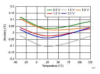
GUID-D34F2D3A-70B5-4552-9116-5108D522B259-low.gif
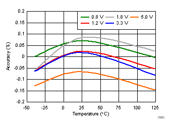
Tested across multiple voltage options
Figure 7-3 Undervoltage Accuracy vs Temperature
GUID-B4E9AFF1-E3EA-4FF3-9CBA-B6BABD5AA921-low.gif
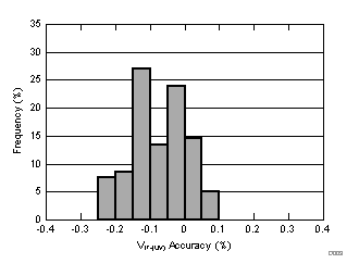
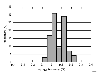
Sample Size of 100 TPS3703A7125 units
Figure 7-5 Undervoltage Accuracy Distribution
GUID-5BEF2B7F-6B4D-4862-A554-0DE9835FBEF6-low.gif
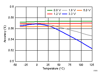
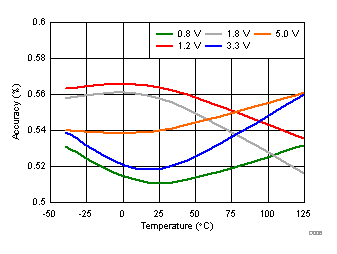
Tested across multiple voltage options
Figure 7-7 Undervoltage Hysteresis Voltage Accuracy vs Temperature
GUID-BC087FB9-3E75-4F6C-965C-258A2DE22253-low.gif
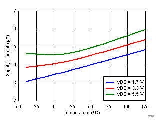
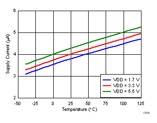
Output ( RESET Pin) = High
Figure 7-9 Supply Current vs Temperature
GUID-2D6A7606-5B90-4AE4-8451-81929DF45DB6-low.gif
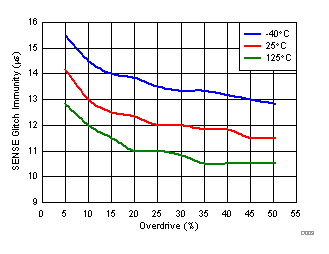
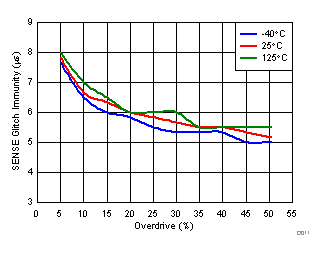
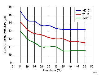
VDD = 1.7 V
Figure 7-11 SENSE Glitch Immunity (VIT-) vs Overdrive
GUID-7B8DF293-84E5-4253-BB12-BDE445D1E189-low.gif
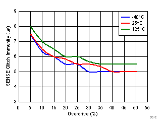
VDD = 5.5 V
Figure 7-13 SENSE Glitch Immunity (VIT-) vs Overdrive
GUID-AE01764D-9961-4191-BB32-F48B35E42FFA-low.gif
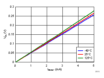
VDD = 1.7 V
Figure 7-15 Low-Level Output Voltage vs RESET current
GUID-F3515F73-37FA-42A7-B43D-21A90E09AF3A-low.gif
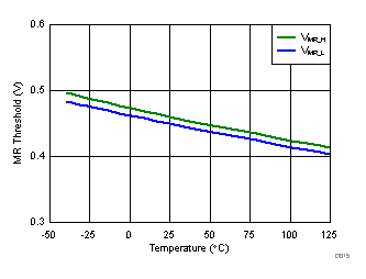
VDD = 1.7 V
Figure 7-17 SET Threshold vs Temperature
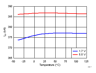
GUID-B1E1D85F-C0C3-4E66-BD88-F1BB72636CCD-low.gif
Figure 7-19 CT Current vs CT value
GUID-DB1D5EA3-D74D-41F9-BBA3-BC3900A7E0AA-low.gif
Figure 7-21 Timeout vs CT Capacitor (0.1 to 10 nF)
GUID-AA28EB87-A6E6-4189-B7F2-85A824C7D890-low.gif
Tested across multiple voltage options
Figure 7-4 Overvoltage Accuracy vs Temperature
GUID-C084FD53-C357-4E21-A85C-F6C96C4DEA79-low.gif
Sample Size of 100 TPS3703A7125 units
Figure 7-6 Overvoltage Accuracy Distribution
GUID-18AE0570-D2D5-4B89-9245-02A64B5C58B3-low.gif
Tested across multiple voltage options
Figure 7-8 Overvoltage Hysteresis Voltage Accuracy vs Temperature
GUID-754792AC-1C6C-4971-9D06-05B6C9933FBF-low.gif
Output ( RESET Pin) = Low
Figure 7-10 Supply Current vs Temperature
GUID-4BA1DA92-195A-4768-809F-76C1FE3BBEE4-low.gif
VDD = 1.7 V
Figure 7-12 SENSE Glitch Immunity (VIT+) vs Overdrive
GUID-959D1E58-44CE-4AFF-9BC0-354E74FFD7C3-low.gif
VDD = 5.5 V
Figure 7-14 SENSE Glitch Immunity (VIT+) vs Overdrive
GUID-8DF894B6-90EC-4665-A345-4A40E2CA1B46-low.gif
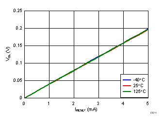
VDD = 5.5 V
Figure 7-16 Low-Level Output Voltage vs RESET current
GUID-FFB74A69-79DB-46D8-8492-7CFB9CB13507-low.gif
VDD = 5.5 V
Figure 7-18 SET Threshold vs Temperature
GUID-52B97310-4340-49DC-9496-88EA81FDE8F9-low.gif
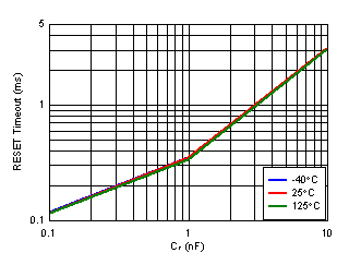
Figure 7-20 RESET Timeout vs CT Capacitor
GUID-94000A70-BF5E-41B9-9905-D7C32630A832-low.gif
Figure 7-22 Detect Propagation Delay vs Temperature