ZHCSL89B may 2020 – november 2020 TPS3703
PRODUCTION DATA
- 1
- 1 特性
- 2 应用
- 3 说明
- 4 Revision History
- 5 Device Comparison
- 6 Pin Configuration and Functions
- 7 Specifications
- 8 Detailed Description
- 9 Application and Implementation
- 10Power Supply Recommendations
- 11Layout
- 12Device and Documentation Support
- 13Mechanical, Packaging, and Orderable Information
9.1.4 Adjustable Voltage Thresholds
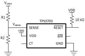
The TPS3703 0.7% maximum accuracy allows for adjustable voltage thresholds using external resistors without adding major inaccuracies to the device. In case that the desired monitored voltage is not available, external resistor dividers can be used to set the desired voltage thresholds. Figure 9-4 illustrates an example of how to adjust the voltage threshold with external resistor dividers. The resistors can be calculated depending on the desired voltage threshold and device part number. TI recommends using the 0.8V voltage threshold device such as the TPS3703B3080 because of the bypass mode of internal resistor ladder.
For example, consider a 2.0 V rail being monitored (VMON) using the TPS3703B3080 variant. Using Equation 4, R1 = 15 kΩ given that R2 = 10 kΩ, VMON = 2 V, and VSENSE = 0.8 V. This device is typically meant to monitor a 0.8 V rail with ±3% voltage thresholds. This means that the device undervoltage threshold (VIT-(UV)) and overvoltage threshold (VIT-(OV)) is 0.776 V and 0.824 V respectively. Using Equation 4, VMON = 1.94 V when VSENSE = VIT-(UV). This can be denoted as VMON-, the monitored undervoltage threshold where the device will assert a reset signal. Using Equation 4 again, the monitored overvoltage threshold (VMON+) = 2.06 V when VSENSE = VIT+(OV). If a wider tolerance or UV only threshold is desired, use a device variant shown on Table 12-1 to determine what device part number matches your application.
There are inaccuracies that must be taken into
consideration while adjusting voltage thresholds. Aside from the tolerance of the
resistor divider, there is an internal resistance of the SENSE pin that may affect
the accuracy of the resistor divider. Although expected to be very high impedance,
users are recommended to calculate the values for design specifications. The
internal sense resistance (RSENSE) can be calculated by the sense voltage
(VSENSE) divided by the sense current (ISENSE) as shown in
Equation 6. VSENSE can be calculated using
Equation 4 depending on the resistor divider and monitored voltage. ISENSE can be
calculated using Equation 5.
 Figure 9-4 Adjustable Voltage Threshold with External Resistor Dividers