ZHCSED3B November   2015  – December 2023 TPS3711

PRODUCTION DATA  

  1.   1
  2. 特性
  3. 应用
  4. 说明
  5. Pin Configuration and Functions
  6. Specifications
    1. 5.1 Absolute Maximum Ratings #GUID-795AD25B-5DDA-4725-83BA-87F5B93DF96A/ABSMAXNOTE
    2. 5.2 ESD Ratings
    3. 5.3 Recommended Operating Conditions
    4. 5.4 Thermal Information
    5. 5.5 Electrical Characteristics
    6. 5.6 Timing Requirements
    7. 5.7 Typical Characteristics
  7. Detailed Description
    1. 6.1 Overview
    2. 6.2 Functional Block Diagram
    3. 6.3 Feature Description
      1. 6.3.1 Input Pin (SENSE)
      2. 6.3.2 Output Pin (OUT)
    4. 6.4 Device Functional Modes
      1. 6.4.1 Normal Operation (VDD > UVLO)
      2. 6.4.2 Undervoltage Lockout (V(POR) < VDD < UVLO)
      3. 6.4.3 Power On Reset (VDD < V(POR))
  8. Application and Implementation
    1. 7.1 Application Information
      1. 7.1.1 Input and Output Configurations
      2. 7.1.2 Immunity to Input Pin Voltage Transients
    2. 7.2 Typical Application
      1. 7.2.1 Design Requirements
      2. 7.2.2 Detailed Design Procedure
        1. 7.2.2.1 Resistor Divider Selection
        2. 7.2.2.2 Pullup Resistor Selection
        3. 7.2.2.3 Input Supply Capacitor
      3. 7.2.3 Application Curves
    3. 7.3 Power Supply Recommendations
    4. 7.4 Layout
      1. 7.4.1 Layout Guidelines
      2. 7.4.2 Layout Example
  9. Device and Documentation Support
    1. 8.1 Documentation Support
      1. 8.1.1 Related Documentation
    2. 8.2 支持资源
    3. 8.3 Trademarks
    4. 8.4 静电放电警告
    5. 8.5 术语表
  10. Revision History
  11. 10Mechanical, Packaging, and Orderable Information

封装选项

机械数据 (封装 | 引脚)
散热焊盘机械数据 (封装 | 引脚)
订购信息

Typical Characteristics

at TJ = 25°C and VDD = 12 V (unless otherwise noted)
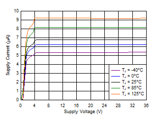
GUID-5CCC3481-AAAD-4277-A26B-ABD39E7D67AB-low.gif
Figure 5-2 Supply Current vs Supply Voltage
GUID-531CB01D-C630-46AF-A3C6-565FAFB8F767-low.gif
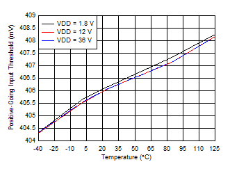
Figure 5-4 SENSE Positive Input Threshold Voltage (VIT+) vs Temperature
GUID-82B806E9-D1C4-445C-8933-8FA951128226-low.gif
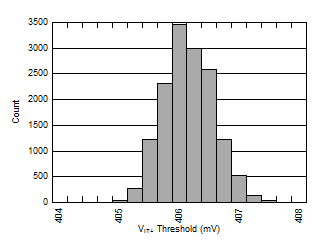
VDD = 1.8 V
Figure 5-6 SENSE Positive Input Threshold Voltage (VIT+) Distribution
GUID-3587E170-CE5C-44D9-BC00-58FB0450E21A-low.gif
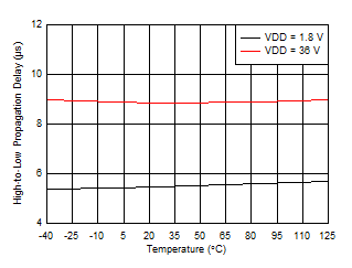
Input step ±200 mV
Figure 5-8 Propagation Delay vs Temperature (High-to-Low Transition at SENSE)
GUID-530104E3-7551-4F79-9155-45AA2080BA55-low.gif
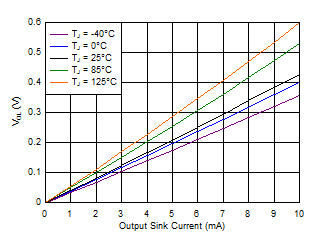
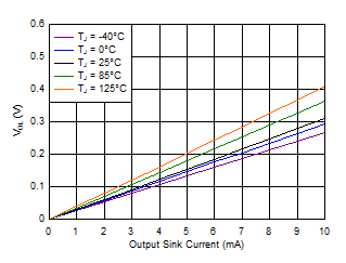
VDD = 1.8 V
Figure 5-10 Output Voltage Low vs Output Sink Current
GUID-8FD7B2F2-598D-47BC-AD08-DD43948EDC20-low.gif
VDD = 5 V
Figure 5-12 Startup Delay vs Temperature
GUID-75D6A6D9-3145-437A-B3EA-2457DAC19F73-low.gif
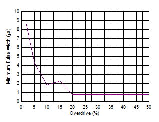
VDD = 24 V, minimum pulse duration required to trigger output high-to-low transition, SENSE = negative spike below VIT–
Figure 5-3 Minimum Pulse Duration vs Threshold Overdrive Voltage
GUID-02729D8F-02F6-4625-84BD-310BC5458C7A-low.gif
Figure 5-5 SENSE Negative Input Threshold Voltage (VIT–) vs Temperature
GUID-B3841321-EDD5-41C9-A712-4C9ECB984E64-low.gif
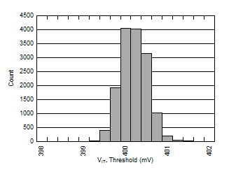
VDD = 1.8 V
Figure 5-7 SENSE Negative Input Threshold Voltage (VIT–) Distribution
GUID-29FA4C34-ADF2-41E6-AEC9-7E89BE5EC34C-low.gif
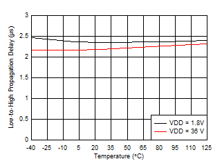
Input step ±200 mV
Figure 5-9 Propagation Delay vs Temperature (Low-to-High Transition at SENSE)
GUID-9C327011-9823-4DF0-B304-76773B82B5A2-low.gif
VDD = 12 V
Figure 5-11 Output Voltage Low vs Output Sink Current