-
TPS3808Gxx-Q1 Low-Quiescent-Current Programmable-Delay Supervisory Circuit
- 1 Features
- 2 Applications
- 3 Description
- 4 Revision History
- 5 Device Comparison Table
- 6 Pin Configuration and Functions
- 7 Specifications
- 8 Detailed Description
- 9 Applications and Implementation
- 10Power Supply Recommendations
- 11Layout
- 12Device and Documentation Support
- 13Mechanical, Packaging, and Orderable Information
- IMPORTANT NOTICE
封装选项
机械数据 (封装 | 引脚)
散热焊盘机械数据 (封装 | 引脚)
- DRV|6
订购信息
TPS3808Gxx-Q1 Low-Quiescent-Current Programmable-Delay Supervisory Circuit
1 Features
- Qualified for Automotive Applications
- Power-On Reset Generator With Adjustable Delay Time: 1.25 ms to 10 s
- Very Low Quiescent Current: 2.4 μA Typical
- High Threshold Accuracy: 0.5% Typical
- Fixed Threshold Voltages for Standard Voltage Rails From 1.2 V to 5 V and Adjustable Voltage Down to 0.4 V Are Available
- Manual Reset (MR) Input
- Open-Drain RESET Output
- Temperature Range: –40°C to +125°C
- Small SOT-23 Package and WSON Package (TPS3808G01QDRVRQ1 only)
2 Applications
- DSP or Microcontroller Applications
- FPGA and ASIC Applications
- Automotive Vision
- Automotive Radar
3 Description
The TPS3808Gxx-Q1 microprocessor supervisory circuits monitor system voltages from 0.4 V to 5 V, asserting an open-drain RESET signal when the SENSE voltage drops below a preset threshold or when the manual reset (MR) pin drops to a logic low. The RESET output remains low for the user-adjustable delay time after the SENSE voltage and MR return above their thresholds.
The TPS3808Gxx-Q1 device uses a precision reference to achieve 0.5% threshold accuracy for VIT ≤ 3.3 V. The reset delay time can be set to 20 ms by disconnecting the CT pin, 300 ms by connecting the CT pin to VDD using a resistor, or can be user-adjusted from 1.25 ms to 10 s by connecting the CT pin to an external capacitor. The TPS3808Gxx-Q1 has a very low typical quiescent current of 2.4 μA, so it is well suited for battery-powered applications. The device is available in a small SOT-23 package (one option available in WSON) and is fully specified over a temperature range of –40°C to +125°C (TJ).
For more information about TI's voltage supervisor portfolio, visit the Supervisor and Reset IC Overview Page page.
Device Information(1)
| PART NUMBER | PACKAGE | BODY SIZE (NOM) |
|---|---|---|
| TPS3808Gxx-Q1 | SOT-23 (6) | 2.90 mm × 1.60 mm |
| WSON (6) | 2.00 mm × 2.00 mm |
- For all available packages, see the orderable addendum at the end of the data sheet.
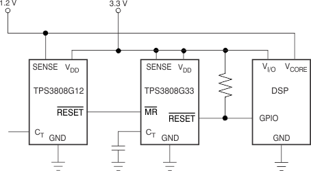
Typical Application Schematic
4 Revision History
Changes from I Revision (June 2015) to J Revision
- Added column for WSON pins Go
- Changed unit for last row of td row in Timing Requirements from "ms" to "s" and "TYP" to "NOM" in middle unit columnGo
Changes from H Revision (June 2012) to I Revision
- Added ESD Ratings table, Feature Description section, Device Functional Modes, Application and Implementation section, Power Supply Recommendations section, Layout section, Device and Documentation Support section, and Mechanical, Packaging, and Orderable Information section Go
Changes from G Revision (November, 2010) to H Revision
- Changed ISENSE from µA to nAGo
5 Device Comparison Table
| ORDERABLE PART NUMBER | NOMINAL SUPPLY VOLTAGE | THRESHOLD VOLTAGE (VIT) |
|---|---|---|
| TPS3808G01QDRVRQ1 | Adjustable | 0.405 V |
| TPS3808G01QDBVRQ1 | ||
| TPS3808G12QDBVRQ1 | 1.2 V | 1.12 V |
| TPS3808G125QDBVRQ1 | 1.25 V | 1.16 V |
| TPS3808G15QDBVRQ1 | 1.5 V | 1.4 V |
| TPS3808G18QDBVRQ1 | 1.8 V | 1.67 V |
| TPS3808G30QDBVRQ1 | 3 V | 2.79 V |
| TPS3808G33QDBVRQ1 | 3.3 V | 3.07 V |
| TPS3808G50QDBVRQ1 | 5 V | 4.65 V |
6 Pin Configuration and Functions
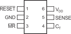

Pin Functions
| PIN | I/O | DESCRIPTION | ||
|---|---|---|---|---|
| NAME | SOT-23 | WSON | ||
| CT | 4 | 3 | I | Reset period programming pin. Connecting this pin to VDD through a 40-kΩ to 200-kΩ resistor or leaving it open results in fixed delay times (see Electrical Characteristics). Connecting this pin to a ground referenced capacitor ≥ 100 pF gives user-programmable delay time. See the Selecting the Reset Delay Time for more information. |
| GND | 2 | 5 | — | Ground |
| MR | 3 | 4 | I | Manual reset. Driving this pin low asserts RESET. MR is internally tied to VDD by a 90-kΩ pullup resistor. |
| RESET | 1 | 6 | O | Reset. This is an open-drain output that is driven to a low impedance state when RESET is asserted (either the SENSE input is lower than the threshold voltage (VIT) or the MR pin is set to a logic low). RESET remains low (asserted) for the reset period after both SENSE is above VIT and MR is set to a logic high. A pullup resistor from 10 kΩ to 1 MΩ must be used on this pin and allows the reset pin to attain voltages higher than VDD. |
| SENSE | 5 | 2 | I | Voltage sense. This pin is connected to the voltage to be monitored. If the voltage at this terminal drops below the threshold voltage (VIT), RESET is asserted. |
| VDD | 6 | 1 | I | Supply voltage. It is good analog design practice to place a 0.1-μF ceramic capacitor close to this pin. |
| Thermal Pad | — | Pad | — | Thermal pad; connect to ground plan to enhance thermal performance of the package. |
7 Specifications
7.1 Absolute Maximum Ratings
over operating junction temperature range (unless otherwise noted)(1)| MIN | MAX | UNIT | ||||
|---|---|---|---|---|---|---|
| VDD | Input voltage | –0.3 | 7 | V | ||
| VCT | CT voltage | –0.3 | (VDD + 0.3) | V | ||
| VMR, VRESET, VSENSE |
MR, RESET, SENSE voltage | –0.3 | 7 | V | ||
| IRESET | RESET pin current | 5 | mA | |||
| TJ | Operating junction temperature(2) | –40 | 150 | °C | ||
| Tstg | Storage temperature | –65 | 150 | °C | ||
7.2 ESD Ratings
| VALUE | UNIT | ||||||
|---|---|---|---|---|---|---|---|
| TPS3808G125QDBVRQ1 IN SOT-23 PACKAGE | |||||||
| V(ESD) | Electrostatic discharge | Human body model (HBM), per AEC Q100-002(1) | ±2000 | V | |||
| Charged device model (CDM), per AEC Q100-011 | ±1000 | ||||||
| Machine Model (MM) | ±50 | ||||||
| TPS3808GXX-Q1 IN SOT-23 PACKAGE | |||||||
| V(ESD) | Electrostatic discharge | Human body model (HBM), per AEC Q100-002(1) | ±2000 | V | |||
| Charged device model (CDM), per AEC Q100-011 | ±500 | ||||||
| TPS3808G01QDRVRQ1 IN SON PACKAGE | |||||||
| V(ESD) | Electrostatic discharge | Human body model (HBM), per AEC Q100-002(1) | ±2000 | V | |||
| Charged device model (CDM), per AEC Q100-011 | ±500 | ||||||
| Machine Model (MM) | ±50 | ||||||
7.3 Recommended Operating Conditions
over operating free-air temperature range (unless otherwise noted)| MIN | NOM | MAX | UNIT | ||
|---|---|---|---|---|---|
| VDD input supply | 1.8 | 6.5 | V | ||
| VSENSE SENSE pin voltage | 0 | VDD | V | ||
| MR Manual reset pin voltage | 0 | VDD | V | ||
7.4 Thermal Information
| THERMAL METRIC(1) | TPS3808Gxx-Q1 | UNIT | ||
|---|---|---|---|---|
| DBV (SOT-23) | DRV (WSON) | |||
| 6 PINS | 6 PINS | |||
| RθJA | Junction-to-ambient thermal resistance | 180.9 | 178.1 | °C/W |
| RθJC(top) | Junction-to-case (top) thermal resistance | 117.8 | 95.6 | °C/W |
| RθJB | Junction-to-board thermal resistance | 27.8 | 135 | °C/W |
| ψJT | Junction-to-top characterization parameter | 18.9 | 6.3 | °C/W |
| ψJB | Junction-to-board characterization parameter | 27.3 | 136.6 | °C/W |
| RθJC(bot) | Junction-to-case (bottom) thermal resistance | N/A | 7.3 | °C/W |
7.5 Electrical Characteristics
1.8 V ≤ VDD ≤ 6.5 V, RLRESET = 100 kΩ, CLRESET = 50 pF, over operating temperature range (TJ = –40°C to +125°C) (unless otherwise noted), typical values at TJ = 25°C| PARAMETER | TEST CONDITIONS | MIN | TYP | MAX | UNIT | ||
|---|---|---|---|---|---|---|---|
| VDD | Input supply range | 1.8 | 6.5 | V | |||
| IDD | Supply current (into VDD pin) | VDD = 3.3 V, RESET not asserted, MR, RESET, CT open | 2.4 | 5 | μA | ||
| VDD = 6.5 V, RESET not asserted, MR, RESET, CT open | 2.7 | 6 | |||||
| VOL | Low-level output voltage | 1.3 V ≤ VDD < 1.8 V, IOL = 0.4 mA | 0.3 | V | |||
| 1.8 V ≤ VDD ≤ 6.5 V, IOL = 1 mA | 0.4 | ||||||
| Power-up reset voltage(1) | VOL (max) = 0.2 V, I RESET = 15 μA | 0.8 | V | ||||
| VIT | Negative-going input threshold accuracy | TPS3808G01-Q1 | –2% | ±1% | 2% | ||
| VIT ≤ 3.3 V | –1.5% | ±0.5% | 1.5% | ||||
| 3.3 V < VIT ≤ 5 V | –2% | ±1% | 2% | ||||
| VIT ≤ 3.3 V | –40°C < TJ < 85°C | –1.25% | ±0.5% | 1.25% | |||
| 3.3 V < VIT ≤ 5 V | –1.5% | ±0.5% | 1.5% | ||||
| VHYS | Hysteresis on VIT pin | TPS3808G01-Q1 | 1.5 | 3 | %VIT | ||
| –40°C < TJ < 85°C | 1 | 2 | |||||
| 1 | 2.5 | ||||||
| R MR | MR internal pullup resistance | VSENSE = VIT | 70 | 90 | kΩ | ||
| ISENSE | Input current at SENSE pin | TPS3808G01-Q1 | –25 | 25 | nA | ||
| VSENSE = 6.5 V | 1.7 | μA | |||||
| IOH | RESET leakage current | V RESET = 6.5 V, RESET not asserted | 300 | nA | |||
| CIN | Input capacitance, any pin | CT pin | VIN = 0 V to VDD | 5 | pF | ||
| Other pins | VIN = 0 V to 6.5 V | 5 | |||||
| VIL | MR logic low input | 0 | 0.3 VDD | V | |||
| VIH | MR logic high input | 0.7 VDD | VDD | V | |||
7.6 Timing Requirements
| MIN | NOM | MAX | UNIT | ||||
|---|---|---|---|---|---|---|---|
| td | RESET delay time | CT = Open | See Figure 1 | 12 | 20 | 28 | ms |
| CT = VDD | 180 | 300 | 420 | ||||
| CT = 100 pF | 0.75 | 1.25 | 1.75 | ||||
| CT = 180 nF | 0.7 | 1.2 | 1.7 | s | |||
| tpHL | Propagation delay | MR to RESET | VIH = 0.7 VDD, VIL = 0.3 VDD | 150 | ns | ||
| High-level to low-level RESET delay | SENSE to RESET | VIH = 1.05 VIT, VIL = 0.95 VIT | 20 | μs | |||
| tw | Maximum transient duration | SENSE | VIH = 1.05 VIT, VIL = 0.95 VIT | 20 | μs | ||
| MR | VIH = 0.7 VDD, VIL = 0.3 VDD | 0.001 | |||||
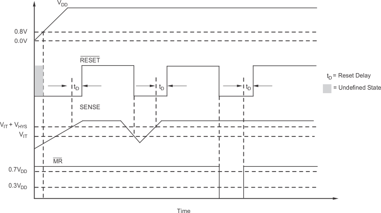 Figure 1. MR and SENSE Reset Timing Diagram
7.7 Typical Characteristics
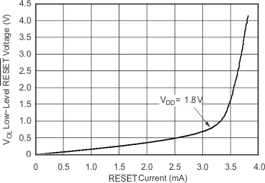
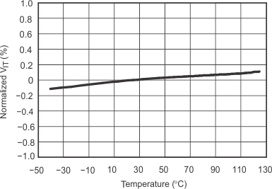
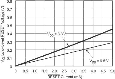
At TJ = 25°C, VDD = 3.3 V, RLRESET = 100 kΩ, and CLRESET = 50 pF (unless otherwise noted)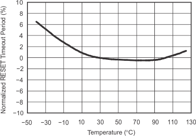
8 Detailed Description
8.1 Overview
The TPS3808Gxx-Q1 devices are low-current supervisory circuits used to monitor system voltages ranging from
0.4 V to 5 V. The devices assert an active low, open-drain RESET signal when the SENSE voltage drops below a preset threshold or when the manual reset (MR) pin is asserted to a logic low. The RESET output remains low for the user-adjustable delay time after the SENSE voltage and MR return above their thresholds. The devices are also designed to be immune to short negative transients on the SENSE pin. The reset delay time can be configured by using the CT pin. The delay can be configured to 20 ms by leaving the CT pin floating, it can be configured to 300 ms by connecting the CT pin to VDD using a resistor, or can be configured from 1.25 ms to 10 s by connecting the CT pin to an external capacitor.
8.2 Functional Block Diagrams
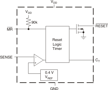
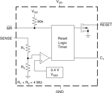 Figure 7. Fixed-Voltage Version
8.3 Feature Description
8.3.1 Immunity to SENSE Pin Voltage Transients
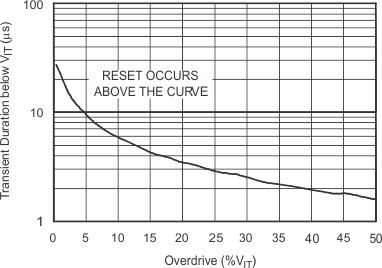
The TPS3808Gxx-Q1 is relatively immune to short negative transients on the SENSE pin. Sensitivity to transients is dependent on threshold overdrive, as shown in the Maximum Transient Duration at Sense vs Sense Threshold Overdrive Voltage graph (Figure 9). This graph shows the duration that the transient is below VIT compared to the magnitude of the voltage drop below VIT, or overdrive voltage. The overdrive voltage is expressed as a percentage of the VIT threshold value. Any combination of transient duration and overdrive voltage that lies above the curve results in RESET being asserted low. Any transient that lies below the curve is ignored by the device.
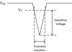 Figure 8. Threshold Overdrive Voltage
8.3.2 SENSE Input
The SENSE input provides a terminal at which any system voltage can be monitored. If the voltage on this pin drops below VIT, RESET is asserted low. The comparator has a built-in hysteresis to ensure smooth RESET assertions and deassertions. It is good analog design practice to put a 1-nF to 10-nF bypass capacitor on the SENSE input to reduce sensitivity to transients and layout parasitics.
The TPS3808G01-Q1 can be used to monitor any voltage rail down to 0.405 V using the circuit shown in Figure 10.
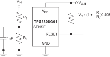 Figure 10. Using the TPS3808G01-Q1 to Monitor a User-Defined Threshold Voltage
8.3.3 Manual Reset (MR) Input
The manual reset (MR) input allows a processor or other logic circuits to initiate a reset. A logic low (0.3 VDD) on MR causes RESET to assert low. After MR returns to a logic high and SENSE is above its reset threshold, RESET is deasserted high after the user-defined reset delay expires. MR is internally tied to VDD using a 90-kΩ resistor, so this pin can be left unconnected if MR is not used.
See Figure 11 for how MR can be used to monitor multiple system voltages. If the logic signal driving MR does not go fully to VDD, there will be some additional current draw into VDD as a result of the internal pullup resistor on MR. To minimize current draw, a logic-level FET can be used as shown in Figure 12.
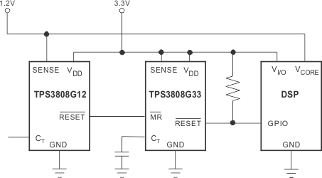 Figure 11. Using MR to Monitor Multiple System Voltages
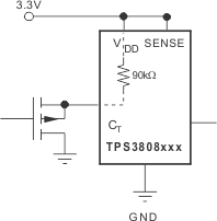 Figure 12. Using an External MOSFET to Minimize IDD When MR Signal Does Not Go to VDD
8.3.4 Selecting the Reset Delay Time
The TPS3808Gxx-Q1 device has three options for setting the RESET delay time as shown in Figure 13. Figure 13 (a) shows the configuration for a fixed 300-ms typical delay time by tying CT to VDD; a resistor from 40 kΩ to 200 kΩ must be used. Supply current is not affected by the choice of resistor. Figure 13 (b) shows a fixed 20-ms delay time by leaving the CT pin open. Figure 13 (c) shows a ground referenced capacitor connected to CT for a user-defined program time from 1.25 ms to 10 s.
 Figure 13. Configuration Used to Set the RESET Delay Time
The capacitor CT should be ≥100 pF nominal value for the TPS3808Gxx-Q1 to recognize the capacitor is present. Use Equation 1 to calculate the capacitor value for a given delay time.

The reset delay time is determined by the time it takes an on-chip precision 220-nA current source to charge the external capacitor to 1.23 V. When RESET asserts low, the capacitor is discharged. When the RESET conditions are cleared, the internal current source is enabled and begins to charge the external capacitor. When the voltage on this capacitor reaches 1.23 V, RESET deasserts. A low-leakage type capacitor such as a ceramic should be used and that stray capacitance around this pin may cause errors in the reset delay time.
8.4 Device Functional Modes
Whenever MR pin is set to a logic high and the SENSE input pin is higher than VIT, the open-drain RESET signal is deasserted high. If MR pin is set to a logic low or the SENSE input pin falls lower than VIT, then RESET is asserted low. Table 1 is a truth table that describes these operating modes.
Table 1. Truth Table
| MR | SENSE > VIT | RESET |
|---|---|---|
| L | 0 | L |
| L | 1 | L |
| H | 0 | L |
| H | 1 | H |