SGLS143D December   2002  – July 2019 TPS3820-Q1 , TPS3823-Q1 , TPS3824-Q1 , TPS3825-Q1 , TPS3828-Q1

PRODUCTION DATA.  

  1. Features
  2. Applications
  3. Description
    1.     Device Images
      1.      Typical Application Schematic
      2.      Normalized Input Threshold Voltage vs Free-Air Temperature
  4. Revision History
  5. Device Comparison Table
  6. Pin Configuration and Functions
    1.     Pin Functions
  7. Specifications
    1. 7.1 Absolute Maximum Ratings
    2. 7.2 ESD Ratings
    3. 7.3 Recommended Operating Conditions
    4. 7.4 Thermal Information
    5. 7.5 Electrical Characteristics
    6. 7.6 Timing Requirements
    7. 7.7 Switching Characteristics
    8. 7.8 Typical Characteristics
  8. Detailed Description
    1. 8.1 Overview
    2. 8.2 Functional Block Diagram
    3. 8.3 Feature Description
      1. 8.3.1 Manual Reset (MR)
      2. 8.3.2 Active High or Active Low Output
      3. 8.3.3 Push-Pull or Open-Drain Output
      4. 8.3.4 Watchdog Timer (WDI)
    4. 8.4 Device Functional Modes
  9. Application and Implementation
    1. 9.1 Application Information
    2. 9.2 Typical Applications
      1. 9.2.1 Supply Rail Monitoring with Watchdog Time-out and 200-ms Delay
        1. 9.2.1.1 Design Requirements
        2. 9.2.1.2 Detailed Design Procedure
        3. 9.2.1.3 Application Curve
      2. 9.2.2 Decoupling WDI During Reset Event
  10. 10Power Supply Recommendations
  11. 11Layout
    1. 11.1 Layout Guidelines
    2. 11.2 Layout Example
  12. 12Device and Documentation Support
    1. 12.1 Documentation Support
      1. 12.1.1 Related Documentation
        1. 12.1.1.1 Related Links
    2. 12.2 Receiving Notification of Documentation Updates
    3. 12.3 Community Resources
    4. 12.4 Trademarks
    5. 12.5 Electrostatic Discharge Caution
    6. 12.6 Glossary
  13. 13Mechanical, Packaging, and Orderable Information

封装选项

请参考 PDF 数据表获取器件具体的封装图。

机械数据 (封装 | 引脚)
  • DBV|5
散热焊盘机械数据 (封装 | 引脚)
订购信息

Pin Configuration and Functions

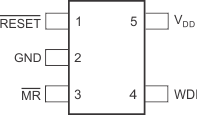
TPS3820-xx-Q1, TPS3823-xx-Q1, TPS3828-xx-Q1: DBV PACKAGE
5-Pin SOT-23
Top View
TPS3820-Q1 TPS3823-Q1 TPS3824-Q1 TPS3825-Q1 TPS3828-Q1 po_dbv_382x_lvs165.gif
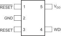
TPS3824-xx-Q1: DBV PACKAGE
5-Pin SOT-23
Top View
TPS3820-Q1 TPS3823-Q1 TPS3824-Q1 TPS3825-Q1 TPS3828-Q1 po_dbv_3824_lvs165.gif
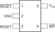
TPS3825-xx-Q1: DBV PACKAGE
5-Pin SOT-23
Top View
TPS3820-Q1 TPS3823-Q1 TPS3824-Q1 TPS3825-Q1 TPS3828-Q1 po_dbv_3825_lvs165.gif

Pin Functions

PIN I/O DESCRIPTION
NAME TPS3820‑xx‑Q1,
TPS3823‑xx‑Q1,
TPS3828‑xx‑Q1
TPS3824‑xx‑Q1 TPS3825‑xx‑Q1
GND 2 2 2 Ground connection
MR 3 4 I Manual-reset input. Pull low to force a reset. RESET remains low as long as MR is low and for the time-out period after MR goes high. Leave unconnected or connect to VDD when unused.
RESET 3 3 O Active-high reset output. Either push-pull or open-drain output stage.
RESET 1 1 1 O Active-low reset output. Either push-pull or open-drain output stage.
VDD 5 5 5 I Supply voltage. Powers the device and monitors its own voltage.
WDI 4 4 I Watchdog timer input. If WDI remains high or low longer than the time-out period, then reset is triggered. The timer clears when reset is asserted or when WDI sees a rising edge or a falling edge. If unused, the WDI connection must be high impedance to prevent it from causing a reset event.