SLVS292F June   2000  – September 2019 TPS3836 , TPS3837 , TPS3838

PRODUCTION DATA.  

  1. Features
  2. Applications
  3. Description
    1.     Device Images
      1.      Typical Application Circuit
  4. Revision History
  5. Device Comparison Table
  6. Pin Configuration and Functions
    1.     Pin Functions
  7. Specifications
    1. 7.1 Absolute Maximum Ratings
    2. 7.2 Dissipation Ratings
    3. 7.3 ESD Ratings
    4. 7.4 Recommended Operating Conditions
    5. 7.5 Thermal Information
    6. 7.6 Electrical Characteristics
    7. 7.7 Timing Requirements
    8. 7.8 Switching Characteristics
    9. 7.9 Typical Characteristics
  8. Parameter Measurement Information
    1. 8.1 Timing Diagram
  9. Detailed Description
    1. 9.1 Overview
    2. 9.2 Functional Block Diagram
    3. 9.3 Feature Description
      1. 9.3.1 Input Voltage (VDD)
      2. 9.3.2 Manual Reset (MR)
      3. 9.3.3 Selectable Reset Delay (CT)
      4. 9.3.4 Reset Output (RESET / RESET)
    4. 9.4 Device Functional Modes
  10. 10Application and Implementation
    1. 10.1 Application Information
    2. 10.2 Typical Application
      1. 10.2.1 Design Requirements
      2. 10.2.2 Detailed Design Procedure
      3. 10.2.3 Application Curves
  11. 11Power Supply Recommendations
  12. 12Layout
    1. 12.1 Layout Guidelines
    2. 12.2 Layout Example
  13. 13Device and Documentation Support
    1. 13.1 Related Links
    2. 13.2 Receiving Notification of Documentation Updates
    3. 13.3 Support Resources
    4. 13.4 Trademarks
    5. 13.5 Electrostatic Discharge Caution
    6. 13.6 Glossary
  14. 14Mechanical, Packaging, and Orderable Information

封装选项

请参考 PDF 数据表获取器件具体的封装图。

机械数据 (封装 | 引脚)
  • DBV|5
  • DRV|6
散热焊盘机械数据 (封装 | 引脚)
订购信息

Typical Characteristics

Test conditions are TJ = 25°C unless otherwise noted.
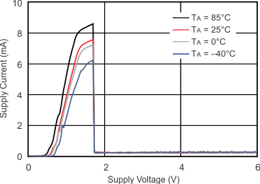
TPS3836 TPS3837 TPS3838 tc_idd-vdd_lvs292.gif
Figure 1. Supply Current vs Supply Voltage
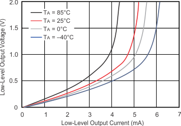
TPS3836 TPS3837 TPS3838 tc_vol-iol_lvs292.gif
Figure 3. Low-Level Output Voltage vs
Low-Level Output Current
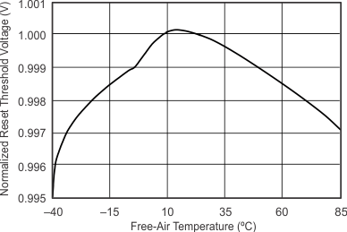
TPS3836 TPS3837 TPS3838 tc_vt-ta_lvs292.gif
Figure 5. Normalized Reset Threshold Voltage vs
Free-Air Temperature
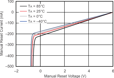
TPS3836 TPS3837 TPS3838 tc_imr-vmr_lvs292.gif
Figure 2. Manual Reset Current vs Manual Reset Voltage
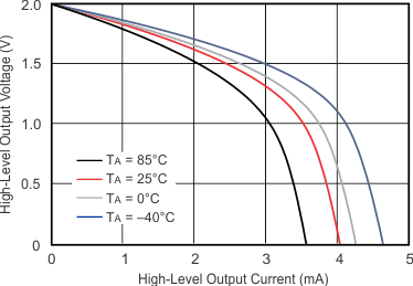
TPS3836 TPS3837 TPS3838 tc_voh-ioh_lvs292.gif
Figure 4. High-Level Output Voltage vs
High-Level Output Current
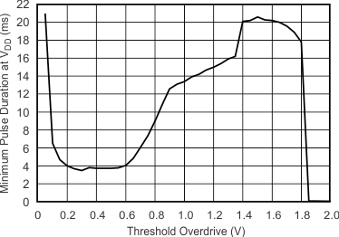
TPS3836 TPS3837 TPS3838 tc_pulse-vdd_lvs292.gif
Figure 6. Minimum Pulse Duration at VDD vs
VDD Threshold Overdrive