SBVS193D June 2012 – July 2015 TPS3831 , TPS3839
PRODUCTION DATA.
- 1 Features
- 2 Applications
- 3 Description
- 4 Revision History
- 5 Device Options
- 6 Pin Configuration and Functions
- 7 Specifications
- 8 Detailed Description
- 9 Applications and Implementation
- 10Power Supply Recommendations
- 11Layout
- 12Device and Documentation Support
- 13Mechanical, Packaging, and Orderable Information
封装选项
机械数据 (封装 | 引脚)
散热焊盘机械数据 (封装 | 引脚)
- DQN|4
订购信息
6 Pin Configuration and Functions
TPS3831 DQN Package
1-mm × 1-mm X2SON
Top View

TPS3839 DQN Package
1-mm × 1-mm X2SON
Top View

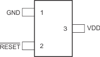
TPS3839 DBZ Package
SOT23-3
Top View

Pin Functions
| PIN | I/O | DESCRIPTION | |||
|---|---|---|---|---|---|
| NAME | NO. | ||||
| TPS3839 (SOT23-3) |
TPS3839 (X2SON) |
TPS3831 (X2SON) |
|||
| GND | 1 | 3 | 3 | — | Ground |
| MR | N/A | N/A | 2 | I | Manual reset. Pull this pin to a logic low to assert the RESET output. After the MR pin is deasserted, the RESET output deasserts after the reset delay (td) elapses. |
| NC | N/A | 2 | N/A | — | No internal connection. |
| RESET | 2 | 1 | 1 | O | Active-low reset output. RESET has a push-pull output drive and is capable of directly driving input pins. RESET is low as long as VDD remains below the factory threshold voltage, and until the delay time (td) elapses after VDD rises above the threshold voltage. |
| Thermal pad | N/A | Available | Available | — | Connect to ground or to a floating copper plane for mechanical stability. |
| VDD | 3 | 4 | 4 | I | Supply voltage |