ZHCSCT8A August 2014 – March 2015 TPS3847
PRODUCTION DATA.
6 Specifications
6.1 Absolute Maximum Ratings(1)
over operating junction temperature range (unless otherwise noted)| MIN | MAX | UNIT | ||
|---|---|---|---|---|
| Voltage | VCC | –0.3 | +20 | V |
| MR | –0.3 | VCC + 0.3 | V | |
| RESET | –0.3 | +5.5 | V | |
| Current | RESET | 10 | mA | |
| Temperature(2) | Operating junction, TJ | –40 | +105 | °C |
| Storage, Tstg | –65 | +150 | °C | |
(1) Stresses beyond those listed under absolute maximum ratings may cause permanent damage to the device. These are stress ratings only, and functional operation of the device at these or any other conditions beyond those indicated under recommended operating conditions is not implied. Exposure to absolute-maximum-rated conditions for extended periods my affect device reliability.
(2) As a result of the low dissipated power in this device, it is assumed that the junction temperature is equal to the ambient temperature.
6.2 ESD Ratings
| VALUE | UNIT | |||
|---|---|---|---|---|
| V(ESD) | Electrostatic discharge | Human-body model (HBM), per ANSI/ESDA/JEDEC JS-001(1) | ±4000 | V |
| Charged-device model (CDM), per JEDEC specification JESD22-C101(2) | ±1500 | |||
(1) JEDEC document JEP155 states that 500-V HBM allows safe manufacturing with a standard ESD control process.
(2) JEDEC document JEP157 states that 250-V CDM allows safe manufacturing with a standard ESD control process.
6.3 Recommended Operating Conditions
over operating junction temperature range (unless otherwise noted)6.4 Thermal Information
| THERMAL METRIC(1) | TPS3847 | UNIT | |
|---|---|---|---|
| DBV (SOT) | |||
| 5 PINS | |||
| RθJA | Junction-to-ambient thermal resistance | 208.5 | °C/W |
| RθJC(top) | Junction-to-case (top) thermal resistance | 123.3 | |
| RθJB | Junction-to-board thermal resistance | 37.2 | |
| ψJT | Junction-to-top characterization parameter | 14.6 | |
| ψJB | Junction-to-board characterization parameter | 36.3 | |
| RθJC(bot) | Junction-to-case (bottom) thermal resistance | N/A | |
(1) For more information about traditional and new thermal metrics, see the IC Package Thermal Metrics application report, SPRA953.
6.5 Electrical Characteristics
At TJ = –40°C to +85°C, 4.5 V < VCC < 18 V, and CIN = 0.1 µF (unless otherwise noted). Typical values are at TJ = 25°C.| PARAMETER | TEST CONDITIONS | MIN | TYP | MAX | UNIT | |||
|---|---|---|---|---|---|---|---|---|
| POWER SUPPLY | ||||||||
| V(VCC) | Input supply voltage range | 4.5 | 18 | V | ||||
| VVO | Minimum V(VCC) voltage for valid output(1) | IOL = 1 µA, VOL = 400 mV | 0.8 | V | ||||
| I(VCC) | Supply current (into VCC pin) | Output not connected | TJ = 25°C, V(VCC) = 18 V | 380 | nA | |||
| TJ = 25°C | 750 | nA | ||||||
| –40°C ≤ TJ ≤ +85°C | 900 | nA | ||||||
| MONITORED THRESHOLD | ||||||||
| VIT– | Negative going input threshold accuracy | TJ = 25°C | ±0.5% | |||||
| –2.5% | +2.5% | |||||||
| Negative-going threshold voltage | TPS3847085 | 8.2875 | 8.5 | 8.7125 | V | |||
| TPS3847108 | 10.53 | 10.8 | 11.07 | V | ||||
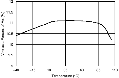
| VHYS | Hysteresis voltage | TPS3847085 | 0.11 × VIT– | V | ||||
| TPS3847108 | 0.035 × VIT– | V | ||||||
| OUTPUT | ||||||||
| VOL | Push-pull low-level output voltage (RESET) | 0.9 V < V(VCC) < 2.4 V, IOL= 10 μA | 0.009 | 0.4 | V | |||
| 2.4 V ≤ V(VCC) < 4.5 V, IOL= 250 μA | 0.015 | 0.4 | V | |||||
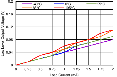
| 4.5 V ≤ V(VCC) ≤ 18 V, IOL= 2 mA | 0.09 | 0.4 | V | |||||
| VOH | Push-pull high-level output voltage (RESET) | IOH = –2 mA | 1.6 | 3.1 | V | |||
| V(VCC) = 18 V | 2.45 | V | ||||||
| IOH = –10 µA | 3 | 4 | V | |||||
| V(VCC) = 18 V | 3.55 | V | ||||||
| MR PIN | ||||||||
| VIL | Low-level input voltage | 0.4 | V | |||||
| VIH | High-level input voltage | 1.2 | V | |||||
| Ilkg(MR) | MR leakage current | MR High, V(VCC) = 18 V | –23 | nA | ||||
(1) The lowest supply voltage (V(VCC)) at which RESET is valid. tRISE(VCC) ≥ 15 µs/V, where tRISE is the rise time.
6.6 Timing Requirements
At TJ = –40°C to +85°C, 4.5 V < VCC < 18 V, and CIN = 0.1 μF (unless otherwise noted). Typical values are at TJ = 25°C.| PARAMETER | MIN | TYP | MAX | UNIT | |
|---|---|---|---|---|---|
| td | RESET delay time(1) | 4.5 | 20 | ms | |
| td(START) | Startup delay time(2) | 6.5 | 40 | ms | |
| tpd(VCC) | Propagation delay for VCC falling(3) | 55 | µs | ||
| tpd(MR) | Propagation delay MR falling(4) | 50 | µs | ||
| tP(MR) | MR minimum high to low pulse duration for RESET low | 50 | µs | ||
(1) Delay from when V(VCC) ≥ VIT– or VMR ≥ VIH until RESET goes high when V(VCC) starts from above the specified minimum V(VCC). Measured with 5% overdrive.
(2) When V(VCC) starts from less than the specified minimum V(VCC) and then exceeds Vth, RESET goes high after the startup delay (td(START)) instead of the RESET delay time (td). Measured with 5% overdrive.
(3) Delay from V(VCC) < Vth until RESET goes low. Measured with 8% overdrive.
(4) Delay from VMR < VIL until RESET goes low. Measured with 8% overdrive.
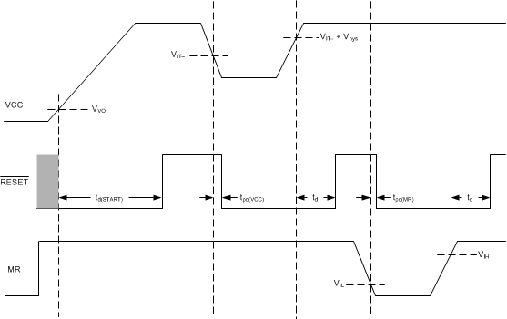 Timing Diagram
6.7 Typical Characteristics
At V(VCC) = 18 V, MR = 1.2 V, RESET = open, and CIN = 0.1 µF (unless otherwise noted).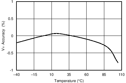
vs Temperature
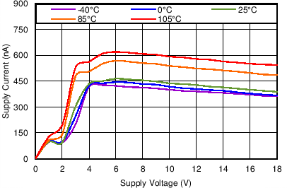
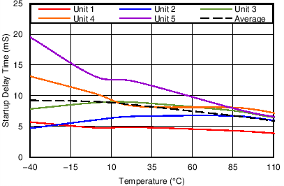
| V(VCC) transitions from 0 V to 10 V | ||
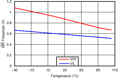
| V(VCC) = 10 V |
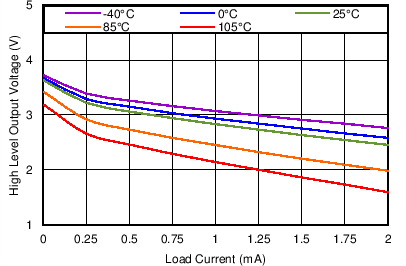
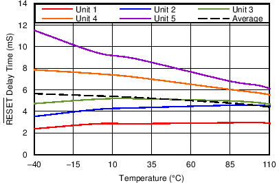
| V(VCC) transitions from 7 V to 10 V | ||
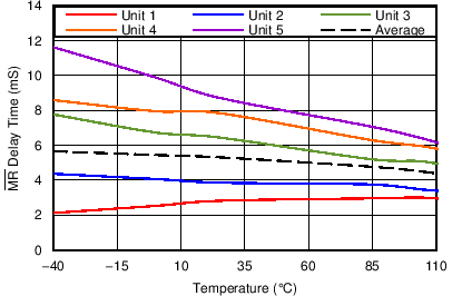
| MR transitions from 0.4 V to 1.2 V, V(VCC) = 10 V | ||
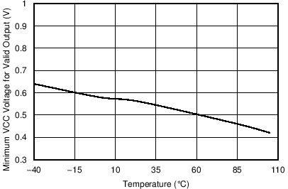
| MR open |
