ZHCSCT8A August 2014 – March 2015 TPS3847
PRODUCTION DATA.
8 Application and Implementation
NOTE
Information in the following applications sections is not part of the TI component specification, and TI does not warrant its accuracy or completeness. TI’s customers are responsible for determining suitability of components for their purposes. Customers should validate and test their design implementation to confirm system functionality.
8.1 Application Information
The TPS3847 family consists of wide-operating voltage, ultralow-current devices that monitor the power-supply voltage. The device asserts an active-low reset signal whenever the supply voltage drops below the factory-trimmed reset. The ultralow current consumption of 380 nA combined with 18-V capability makes the TPS3847 ideal for use in low-power and portable applications.
8.2 Typical Application
Wide operating voltage and threshold options make the TPS3847 well suited for monitoring dual- and triple-cell, lithium-ion battery applications. Figure 15 shows the TPS3847 used to disable a buck converter when the cell voltage discharges below the threshold voltage. When the cell voltage reaches VIT–, the enable pin of the TPS62120 is driven low, placing the buck converter in a low-current, shutdown state.
 Figure 15. Disabled Buck Converter
8.2.1 Design Requirements
8.2.1.1 Input Capacitor
The TPS3847 uses a unique sampling scheme to maintain an extremely low average quiescent current of
380 nA. However, this current rises to approximately 12 µA for approximately 500 µs while the TPS3847 refreshes the reference voltage. This refresh pulse typically occurs every 200 ms. If the source impedance to the supply voltage is high, then the additional current during sampling may trigger a false reset as a result of the voltage drop from the supply to the VCC pin. For sources with a high impedance, or applications with long or thin VCC traces, add a 0.1-µF or larger bypass capacitor near the VCC pin. Adding this bypass capacitor effectively keeps the average current supplied from the input source close to 380 nA, reducing the voltage droop caused by the refresh pulse, and is good analog design practice.
8.2.1.2 Driving Bidirectional Reset Pins
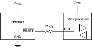
Some microcontrollers have bidirectional reset pins that act as both an input and an output. When using bidirectional reset pins, place a series resistor between the TPS3847 RESET pin and the microcontroller in order to protect against excessive current flow in case both the TPS3847 and the microcontroller attempt to drive the reset line simultaneously. Figure 16 illustrates the connection of the TPS3847 to a microcontroller using a series resistor to drive a bidirectional reset line. Assuming the maximum voltage that the microprocessor outputs is the same as the TPS3847 (4 V), use a resistor value greater than 20 kΩ in order to limit the output current to 2 mA or less when one pin is driven high and the other is driven low. In order to cover the majority of applications, use a resistor value of 47 kΩ.
 Figure 16. Connection to Bidirectional Reset Pin
8.2.1.3 Manual Reset (MR) Input
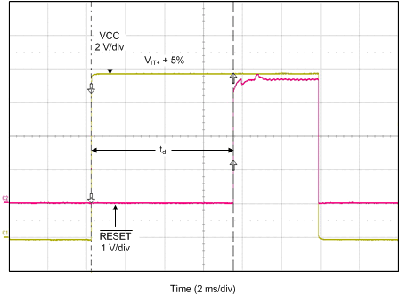
The manual reset (MR) input allows a processor, or other logic devices, to initiate a reset. A logic low on MR causes RESET to transition to logic low. After MR returns to a logic high and V(VCC) is greater than VIT+, RESET transitions to a logic high after the reset delay time, td, elapses.
Note that internal to the device MR is connected to a very small current source that goes from the internal sub-regulated voltage to the MR node. If the logic signal driving MR does not exceed 3 V, there is 25 nA of additional current drawn from the input supply because of this current source. Do not leave this pin floating; either drive this pin above or below the MR high and low input levels. Tie MR directly to VCC if not used.
8.2.1.4 Threshold Overdrive
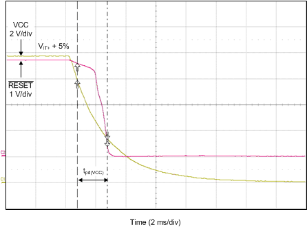
Threshold overdrive is how much V(VCC) exceeds the specified threshold, and is important to know because the smaller the overdrive, the slower the RESET response. Threshold overdrive is calculated as a percent of the threshold in question, as shown in Equation 1:
where
- VIT is either VIT– or VIT+, depending on whether calculating the overdrive for the negative-going threshold or the positive-going threshold, respectively.
Figure 12 illustrates the VCC minimum detectable pulse versus overdrive, and is used to visualize the relationship overdrive has on tpd(VCC) for negative-going events.
For positive-going events, after the overdrive is greater than 5%, the changes to td are negligible because of the significantly longer delay time. When overdrive is less than 5%, td can increase to 200 ms while the device waits for the next voltage reference refresh pulse.
8.2.2 Detailed Design Procedure
● Select desired device based on the threshold voltage.
● Ensure that the trace from the input supply to the VCC pin is low impedance in order to avoid false reset signals during the refresh cycle. If the impedance is too high, add an input capacitor of 0.1-µF or larger close to the VCC pin (see the Input Capacitor section).
● If the RESET of the TPS3847 is driving a bidirectional pin, place a resistor between the output of the TPS3847 and the bidirectional pin (see the Driving Bidirectional Reset Pins section).
8.2.3 Application Curves

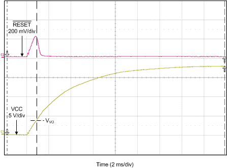
Valid Output


8.3 Do's and Don'ts
Connect a 0.1-µF to 1.0-µF low equivalent series resistance (ESR) capacitor between the VCC pin and the GND pin.
Connect the MR pin to a voltage higher than 1.2 V in order for RESET to go high or low, depending on the value of V(VCC) relative to VIT–.
Connect the MR pin to a voltage lower than 0.4 V in order to hold RESET low, regardless of the value of V(VCC).
Connect the MR pin to the VCC pin if MR functionality is not used.
Do not connect the VCC pin to a high-impedance supply without a 0.1-µF to 1.0-µF low equivalent series resistance (ESR) bypass capacitor.
Do not use a thin, long trace to connect the VCC pin to the input supply without a 0.1-µF to 1.0-µF low ESR bypass capacitor.
Do not leave the MR pin floating.