ZHCSFY8B January   2017  – September 2021 TPS3850-Q1

PRODUCTION DATA  

  1. 特性
  2. 应用
  3. 说明
  4. Revision History
  5. Pin Configuration and Functions
  6. Specifications
    1. 6.1 Absolute Maximum Ratings
    2. 6.2 ESD Ratings
    3. 6.3 Recommended Operating Conditions
    4. 6.4 Thermal Information
    5. 6.5 Electrical Characteristics
    6. 6.6 Timing Requirements
    7. 6.7 Timing Diagrams
    8. 6.8 Typical Characteristics
  7. Detailed Description
    1. 7.1 Overview
    2. 7.2 Functional Block Diagrams
    3. 7.3 Feature Description
      1. 7.3.1 CRST
      2. 7.3.2 RESET
      3. 7.3.3 Over- and Undervoltage Fault Detection
      4. 7.3.4 Adjustable Operation Using the TPS3850H01Q1
      5. 7.3.5 Window Watchdog
        1. 7.3.5.1 SET0 and SET1
          1. 7.3.5.1.1 Enabling the Window Watchdog
          2. 7.3.5.1.2 Disabling the Watchdog Timer When Using the CRST Capacitor
          3. 7.3.5.1.3 SET0 and SET1 During Normal Watchdog Operation
      6. 7.3.6 Window Watchdog Timer
        1. 7.3.6.1 CWD
        2. 7.3.6.2 WDI Functionality
        3. 7.3.6.3 WDO Functionality
    4. 7.4 Device Functional Modes
      1. 7.4.1 VDD is Below VPOR ( VDD < VPOR)
      2. 7.4.2 Above Power-On-Reset But Less Than UVLO (VPOR ≤ VDD < VUVLO)
      3. 7.4.3 Above UVLO But Less Than VDD (min) (VUVLO ≤ VDD < VDD (min))
      4. 7.4.4 Normal Operation (VDD ≥ VDD (min))
  8. Application and Implementation
    1. 8.1 Application Information
      1. 8.1.1 CRST Delay
        1. 8.1.1.1 Factory-Programmed Reset Delay Timing
        2. 8.1.1.2 Programmable Reset Delay Timing
      2. 8.1.2 CWD Functionality
        1. 8.1.2.1 Factory-Programmed Timing Options
        2. 8.1.2.2 Adjustable Capacitor Timing
        3. 8.1.2.3 45
      3. 8.1.3 Adjustable SENSE Configuration
      4. 8.1.4 Overdrive on the SENSE Pin
    2. 8.2 Typical Applications
      1. 8.2.1 Design 1: Monitoring a 1.2-V Rail with Factory-Programmable Watchdog Timing
        1. 8.2.1.1 Design Requirements
        2. 8.2.1.2 Detailed Design Procedure
          1. 8.2.1.2.1 Monitoring the 1.2-V Rail
          2. 8.2.1.2.2 Meeting the Minimum Reset Delay
          3. 8.2.1.2.3 Setting the Watchdog Window
          4. 8.2.1.2.4 Calculating the RESET and WDO Pullup Resistor
        3. 8.2.1.3 Application Curves
      2. 8.2.2 Design 2: Using the TPS3850H01Q1 to Monitor a 0.7-V Rail With an Adjustable Window Watchdog Timing
        1. 8.2.2.1 Design Requirements
        2. 8.2.2.2 Detailed Design Procedure
          1. 8.2.2.2.1 Meeting the Minimum Reset Delay
          2. 8.2.2.2.2 Setting the Window Watchdog
          3. 8.2.2.2.3 Watchdog Disabled During the Initialization Period
          4. 8.2.2.2.4 Calculating the Sense Resistor
        3. 8.2.2.3 Application Curves
  9. Power Supply Recommendations
  10. 10Layout
    1. 10.1 Layout Guidelines
    2. 10.2 Layout Example
  11. 11Device and Documentation Support
    1. 11.1 Device Support
      1. 11.1.1 Development Support
        1. 11.1.1.1 Evaluation Module
      2. 11.1.2 Device Nomenclature
    2. 11.2 Documentation Support
      1. 11.2.1 Related Documentation
    3. 11.3 接收文档更新通知
    4. 11.4 支持资源
    5. 11.5 Trademarks
    6. 11.6 Electrostatic Discharge Caution
    7. 11.7 术语表
  12. 12Mechanical, Packaging, and Orderable Information

封装选项

请参考 PDF 数据表获取器件具体的封装图。

机械数据 (封装 | 引脚)
  • DRC|10
散热焊盘机械数据 (封装 | 引脚)
订购信息

Overdrive on the SENSE Pin

The propagation delay from exceeding the threshold to RESET being asserted is dependent on two conditions: the amplitude of the voltage on the SENSE pin relative to the threshold, (ΔV1 and ΔV2), and the length of time that the voltage is above or below the trip point (t1 and t2). If the voltage is just over the trip point for a long period of time, then RESET asserts and the output is pulled low. However, if the SENSE voltage is just over the trip point for a few nanoseconds, then the RESET does not assert and the output remains high. The time required for RESET to assert can be changed by increasing the time that the SENSE voltage goes over the trip point. Equation 8 shows how to calculate the percentage overdrive.

Equation 8. Overdrive = | ( VSENSE / VITx – 1) × 100% |

In Equation 8, VITx corresponds to the SENSE threshold trip point. If VSENSE exceeds the positive threshold, then VIT+(OV) is used. VIT-(UV) is used when VSENSE falls below the negative threshold. In Figure 8-4, t1 and t2 correspond to the amount of time that the SENSE voltage is over the threshold. The response time versus overdrive for VIT+(OV) and VIT-(UV) is illustrated in Figure 6-14 and Figure 6-17, respectively.

The TPS3850-Q1 is relatively immune to short positive and negative transients on the SENSE pin because of the overdrive voltage curve; see Figure 6-20 and Figure 6-21.
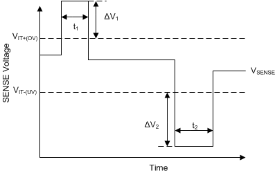
GUID-2AED30EA-DFF9-4DD2-981F-222E1BBEB66C-low.gifFigure 8-4 Overdrive Voltage on the SENSE Pin