ZHCSFP1A November   2016  – September 2021 TPS3851

PRODUCTION DATA  

  1. 特性
  2. 应用
  3. 说明
  4. Revision History
  5. Pin Configuration and Functions
  6. Specifications
    1. 6.1 Absolute Maximum Ratings
    2. 6.2 ESD Ratings
    3. 6.3 Recommended Operating Conditions
    4. 6.4 Thermal Information
    5. 6.5 Electrical Characteristics
    6. 6.6 Timing Requirements
    7. 6.7 Timing Diagrams
    8. 6.8 Typical Characteristics
  7. Detailed Description
    1. 7.1 Overview
    2. 7.2 Functional Block Diagram
    3. 7.3 Feature Description
      1. 7.3.1 RESET
      2. 7.3.2 Manual Reset MR
      3. 7.3.3 UV Fault Detection
      4. 7.3.4 Watchdog Mode
        1. 7.3.4.1 CWD
        2. 7.3.4.2 Watchdog Input WDI
        3. 7.3.4.3 Watchdog Output WDO
        4. 7.3.4.4 SET1
    4. 7.4 Device Functional Modes
      1. 7.4.1 VDD is Below VPOR ( VDD < VPOR)
      2. 7.4.2 Above Power-On-Reset, But Less Than VDD(min) (VPOR ≤ VDD < VDD(min))
      3. 7.4.3 Normal Operation (VDD ≥ VDD(min))
  8. Application and Implementation
    1. 8.1 Application Information
      1. 8.1.1 CWD Functionality
        1. 8.1.1.1 Factory-Programmed Timing Options
        2. 8.1.1.2 Adjustable Capacitor Timing
      2. 8.1.2 Overdrive Voltage
    2. 8.2 Typical Application
      1. 8.2.1 Design Requirements
      2. 8.2.2 Detailed Design Procedure
        1. 8.2.2.1 Monitoring the 1.8-V Rail
        2. 8.2.2.2 Calculating RESET and WDO Pullup Resistor
        3. 8.2.2.3 Setting the Watchdog
        4. 8.2.2.4 Watchdog Disabled During Initialization Period
      3. 8.2.3 Glitch Immunity
      4. 8.2.4 Application Curves
  9. Power Supply Recommendations
  10. 10Layout
    1. 10.1 Layout Guidelines
    2. 10.2 Layout Example
  11. 11Device and Documentation Support
    1. 11.1 Device Support
      1. 11.1.1 Device Nomenclature
    2. 11.2 Documentation Support
      1. 11.2.1 Related Documentation
    3. 11.3 接收文档更新通知
    4. 11.4 支持资源
    5. 11.5 Trademarks
    6. 11.6 Electrostatic Discharge Caution
    7. 11.7 术语表
  12. 12Mechanical, Packaging, and Orderable Information

封装选项

机械数据 (封装 | 引脚)
散热焊盘机械数据 (封装 | 引脚)
订购信息

Watchdog Input WDI

WDI is the watchdog timer input that controls the WDO output. The WDI input is triggered by the falling edge of the input signal. To ensure proper functionality of the watchdog timer, always issue the WDI pulse before tWD(min). If the pulse is issued in this region, then WDO remains unasserted. Otherwise, the device asserts WDO, putting the WDO pin into a low-impedance state.

The watchdog input (WDI) is a digital pin. To ensure there is no increase in IDD, drive the WDI pin to either VDD or GND at all times. Putting the pin to an intermediate voltage can cause an increase in supply current (IDD) because of the architecture of the digital logic gates. When RESET is asserted, the watchdog is disabled and all signals input to WDI are ignored. When RESET is no longer asserted, the device resumes normal operation and no longer ignores the signal on WDI. If the watchdog is disabled, drive the WDI pin to either VDD or GND.
Figure 7-2 shows the valid region for a WDI pulse to be issued to prevent WDO from being triggered and pulled low.
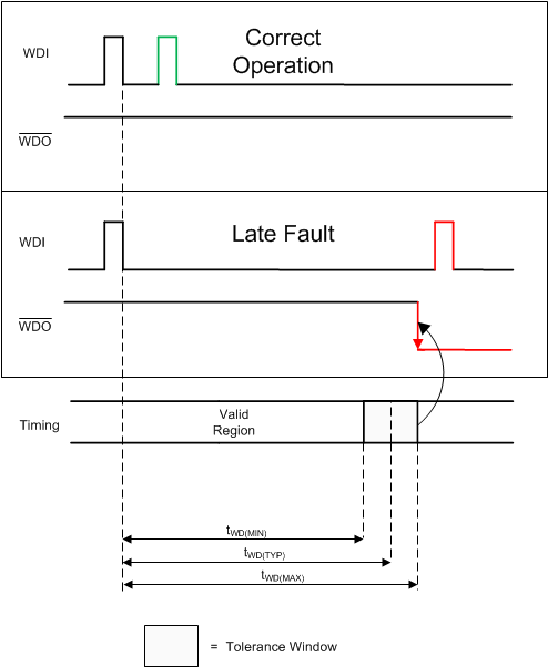
GUID-3C776E44-AD8F-47DE-B973-A10BE0DF0F29-low.gifFigure 7-2 Watchdog Timing Diagram