ZHCSG27 February   2017 TPS3852-Q1

PRODUCTION DATA.  

  1. 特性
  2. 应用
  3. 说明
  4. 修订历史记录
  5. Pin Configuration and Functions
  6. Specifications
    1. 6.1 Absolute Maximum Ratings
    2. 6.2 ESD Ratings
    3. 6.3 Recommended Operating Conditions
    4. 6.4 Thermal Information
    5. 6.5 Electrical Characteristics
    6. 6.6 Timing Requirements
    7. 6.7 Typical Characteristics
  7. Detailed Description
    1. 7.1 Overview
    2. 7.2 Functional Block Diagram
    3. 7.3 Feature Description
      1. 7.3.1 RESET
      2. 7.3.2 Manual Reset (MR)
      3. 7.3.3 Undervoltage Fault Detection
      4. 7.3.4 Watchdog Mode
        1. 7.3.4.1 SET1
        2. 7.3.4.2 Window Watchdog Timer
        3. 7.3.4.3 Watchdog Input (WDI)
        4. 7.3.4.4 CWD
        5. 7.3.4.5 Watchdog Output (WDO)
    4. 7.4 Device Functional Modes
      1. 7.4.1 VDD is Below VPOR (VDD < VPOR)
      2. 7.4.2 Above Power-On-Reset, But Less Than VDD(min) (VPOR ≤ VDD < VDD(min))
      3. 7.4.3 Normal Operation (VDD ≥ VDD(min))
  8. Application and Implementation
    1. 8.1 Application Information
      1. 8.1.1 CWD Functionality
        1. 8.1.1.1 Factory-Programmed Timing Options
        2. 8.1.1.2 Adjustable Capacitor Timing
      2. 8.1.2 Overdrive Voltage
    2. 8.2 Typical Application
      1. 8.2.1 Design Requirements
      2. 8.2.2 Detailed Design Procedure
        1. 8.2.2.1 Monitoring the 3.3-V Rail
        2. 8.2.2.2 Calculating RESET and the WDO Pullup Resistor
        3. 8.2.2.3 Setting the Window Watchdog
        4. 8.2.2.4 Watchdog Disabled During Initialization Period
      3. 8.2.3 Glitch Immunity
      4. 8.2.4 Application Curves
  9. Power Supply Recommendations
  10. 10Layout
    1. 10.1 Layout Guidelines
    2. 10.2 Layout Example
  11. 11器件和文档支持
    1. 11.1 器件支持
      1. 11.1.1 开发支持
        1. 11.1.1.1 评估模块
      2. 11.1.2 器件命名规则
    2. 11.2 接收文档更新通知
    3. 11.3 社区资源
    4. 11.4 商标
    5. 11.5 静电放电警告
    6. 11.6 Glossary
  12. 12机械、封装和可订购信息

封装选项

机械数据 (封装 | 引脚)
散热焊盘机械数据 (封装 | 引脚)
订购信息

Layout

Layout Guidelines

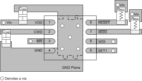
  • Make sure that the connection to the VDD pin is low impedance. Good analog design practice is to place a 0.1-µF ceramic capacitor as near as possible to the VDD pin.
  • If a CCWD capacitor or pull-up resistor is used, place these components as close as possible to the CWD pin. If the CWD pin is left unconnected, make sure to minimize the amount of parasitic capacitance on the pin.
  • Place the pullup resistors on RESET and WDO as close to the pin as possible.

Layout Example

TPS3852-Q1 TPS3851_layout.gif Figure 26. Typical Layout for the TPS3852-Q1