ZHCSG27 February 2017 TPS3852-Q1
PRODUCTION DATA.
- 1 特性
- 2 应用
- 3 说明
- 4 修订历史记录
- 5 Pin Configuration and Functions
- 6 Specifications
- 7 Detailed Description
- 8 Application and Implementation
- 9 Power Supply Recommendations
- 10Layout
- 11器件和文档支持
- 12机械、封装和可订购信息
6 Specifications
6.1 Absolute Maximum Ratings
over operating free-air temperature range (unless otherwise noted)(1)| MIN | MAX | UNIT | ||
|---|---|---|---|---|
| Supply voltage range | VDD | –0.3 | 7 | V |
| Output voltage range | RESET, WDO | –0.3 | 7 | V |
| Voltage ranges | SET1, WDI, MR | –0.3 | 7 | V |
| CWD, CRST | –0.3 | VDD + 0.3(3) | ||
| Output pin current | ±20 | mA | ||
| Input current (all pins) | ±20 | mA | ||
| Continuous total power dissipation | See Thermal Information | |||
| Temperature | Operating junction, TJ(2) | –40 | 150 | °C |
| Operating free-air, TA(2) | –40 | 150 | ||
| Storage, Tstg | –65 | 150 | ||
(1) Stresses beyond those listed under Absolute Maximum Ratings may cause permanent damage to the device. These are stress ratings only, which do not imply functional operation of the device at these or any other conditions beyond those indicated under Recommended Operating Conditions. Exposure to absolute-maximum-rated conditions for extended periods may affect device reliability.
(2) Assume that TJ = TA as a result of the low dissipated power in this device.
(3) The absolute maximum rating is VDD + 0.3 V or 7.0 V, whichever is smaller.
6.2 ESD Ratings
| VALUE | UNIT | ||||
|---|---|---|---|---|---|
| V(ESD) | Electrostatic discharge | Human-body model (HBM), per AEC Q100-002(1) | ±2000 | V | |
| Charged-device model (CDM), per AEC Q100-011 | ±750 | ||||
(1) AEC Q100-002 indicates that HBM stressing shall be in accordance with the ANSI/ESDA/JEDEC JS-001 specification.
6.3 Recommended Operating Conditions
over operating free-air temperature range (unless otherwise noted)| MIN | NOM | MAX | UNIT | ||
|---|---|---|---|---|---|
| VDD | Supply pin voltage | 1.6 | 6.5 | V | |
| VSET1 | SET1 pin voltage | 0 | 6.5 | V | |
| VMR | MR pin voltage | 0 | 6.5 | V | |
| CCWD | Watchdog timing capacitor | 0.1(1) | 1000(1) | nF | |
| CWD | Pullup resistor to VDD | 9 | 10 | 11 | kΩ |
| RPU | Pullup resistor, RESET and WDO | 1 | 10 | 100 | kΩ |
| IRESET | RESET pin current | 10 | mA | ||
| IWDO | Watchdog output current | 10 | mA | ||
| TJ | Junction temperature | –40 | 125 | °C | |
(1) Using a CCWD capacitor of 0.1 nF or 1000 nF gives a tWDU(typ) of 62.74 ms or 77.45 seconds, respectively.
6.4 Thermal Information
| THERMAL METRIC(1) | TPS3852-Q1 | UNIT | |
|---|---|---|---|
| DRB (VSON) | |||
| 8 PINS | |||
| RθJA | Junction-to-ambient thermal resistance | 47.7 | °C/W |
| RθJC(top) | Junction-to-case (top) thermal resistance | 51.5 | °C/W |
| RθJB | Junction-to-board thermal resistance | 22.2 | °C/W |
| ψJT | Junction-to-top characterization parameter | 1.3 | °C/W |
| ψJB | Junction-to-board characterization parameter | 22.3 | °C/W |
| RθJC(bot) | Junction-to-case (bottom) thermal resistance | 4.3 | °C/W |
(1) For more information about traditional and new thermal metrics, see the Semiconductor and IC Package Thermal Metrics application report.
6.5 Electrical Characteristics
at VITN + VHYST ≤ VDD ≤ 6.5 V over the operating temperature range of –40°C ≤ TA, T J ≤ +125°C (unless otherwise noted); the open-drain pullup resistors are 10 kΩ for each output; typical values are at TJ = 25°C| PARAMETER | TEST CONDITIONS | MIN | TYP | MAX | UNIT | |
|---|---|---|---|---|---|---|
| GENERAL CHARACTERISTICS | ||||||
| VDD(3) | Supply voltage | 1.6 | 6.5 | V | ||
| IDD | Supply current | 10 | 19 | µA | ||
| RESET FUNCTION | ||||||
| VPOR(2) | Power-on-reset voltage | IRESET = 15 µA, VOL(MAX) = 0.25 V | 0.8 | V | ||
| VUVLO(1) | Undervoltage lockout voltage | 1.35 | V | |||
| VITN | Undervoltage threshold accuracy, entering RESET |
VDD falling | VITN – 0.8% | VITN + 0.8% | ||
| VHYST | Hysteresis voltage | VDD rising | 0.2% | 0.5% | 0.8% | |
| IMR | MR pin internal pullup current | VMR = 0 V | 500 | 620 | 700 | nA |
| WINDOW WATCHDOG FUNCTION | ||||||
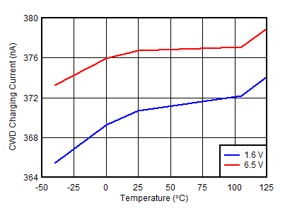
| ICWD | CWD pin charge current | CWD = 0.5 V | 337 | 375 | 413 | nA |
| VCWD | CWD pin threshold voltage | 1.192 | 1.21 | 1.228 | V | |
| VOL | RESET, WDO output low | VDD = 5 V, IRESET = IWDO = 3 mA |
0.4 | V | ||
| ID | RESET, WDO output leakage current, open-drain |
VDD = VITN + VHYST, VRESET = VWDO = 6.5 V |
1 | µA | ||
| VIL | Low-level input voltage (MR, SET1) | 0.25 | V | |||
| VIH | High-level input voltage (MR, SET1) | 0.8 | V | |||
| VIL(WDI) | Low-level input voltage (WDI) | 0.3 × VDD | V | |||
| VIH(WDI) | High-level input voltage (WDI) | 0.8 × VDD | V | |||
(1) When VDD falls below UVLO, RESET is driven low.
(2) When VDD falls below VPOR, RESET and WDO are undefined.
(3) During power on, VDD must be a minimum of 1.6 V for at least 300 µs before RESET correlates with VDD.
6.6 Timing Requirements
at VITN + VHYST ≤ VDD ≤ 6.5 V over the operating temperature range of –40°C ≤ TA, T J ≤ +125°C (unless otherwise noted); the open-drain pullup resistors are 10 kΩ for each output; typical values are at TJ = 25°C| MIN | TYP | MAX | UNIT | |||
|---|---|---|---|---|---|---|
| GENERAL | ||||||
| tINIT | CWD pin evaluation period | 381 | µs | |||
| Minimum MR, SET1 pin pulse duration | 1 | µs | ||||
| Startup delay | 300 | µs | ||||
| RESET FUNCTION | ||||||
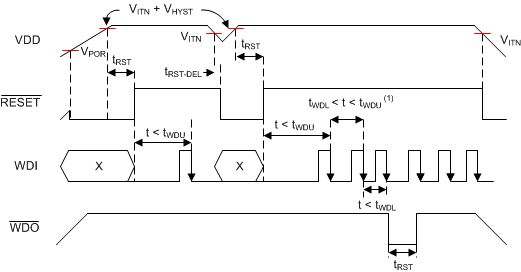
| tRST | Reset timeout period | 170 | 200 | 230 | ms | |
| tRST-DEL | VDD to RESET delay | VDD = VITN + VHYST + 2.5% | 35 | µs | ||
| VDD = VITN – 2.5% | 17 | |||||
| tMR-DEL | MR to RESET delay | 200 | ns | |||
| Watchdog Function | ||||||
| tWDL | Window watchdog lower boundary | CWD = NC, SET1 = 0(1) | Watchdog disabled | |||
| CWD = NC, SET1 = 1(1) | 680 | 800 | 920 | ms | ||
| CWD = 10 kΩ to VDD, SET1 = 0(1) |
Watchdog disabled | |||||
| CWD = 10 kΩ to VDD, SET1 = 1(1) |
1.48 | 1.85 | 2.22 | ms | ||
| tWDU | Window watchdog upper boundary | CWD = NC, SET1 = 0(1) | Watchdog disabled | |||
| CWD = NC, SET1 = 1(1) | 1360 | 1600 | 1840 | ms | ||
| CWD = 10 kΩ to VDD, SET1 = 0(1) |
Watchdog disabled | |||||
| CWD = 10 kΩ to VDD, SET1 = 1(1) |
9.35 | 11.0 | 12.65 | ms | ||
| tWD-setup | Setup time required for device to respond to changes on WDI after being enabled | 150 | µs | |||
| Minimum WDI pulse duration | 50 | ns | ||||
| tWD-DEL | WDI to WDO delay | 50 | ns | |||
(1) SET1 = 0 means VSET1 < VIL, SET1 = 1 means VSET1 > VIH.
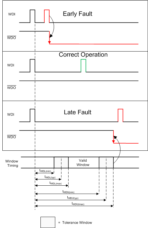 Figure 2. TPS3852-Q1 Window Watchdog Timing
6.7 Typical Characteristics
all curves are taken at 25°C with 1.6 V ≤ VDD ≤ 6.5 V (unless otherwise noted)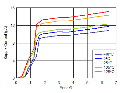
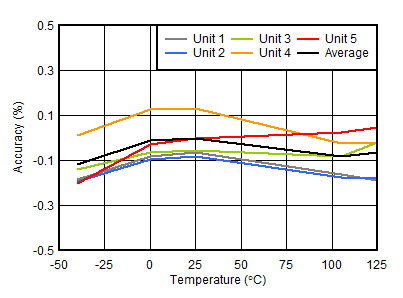
| TPS3852G33-Q1 | ||
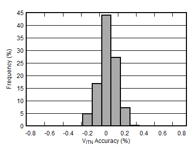
| Includes G and H versions with 3.3-V nominal monitored voltage, total units = 15,536 |
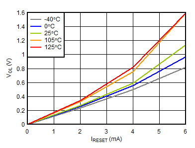
| VDD = 1.6 V |
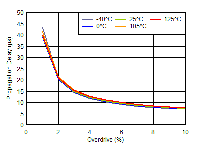
| TPS3852G33-Q1 entering undervoltage |
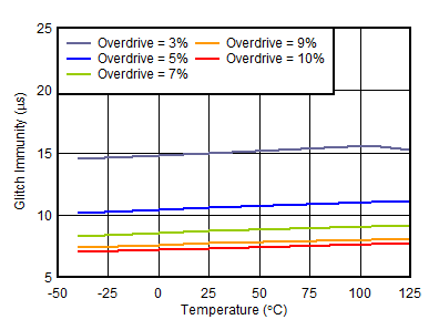
| VITN = 3.168 V |
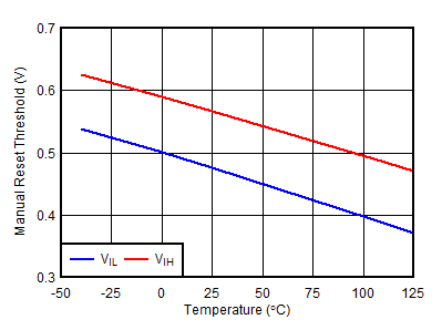
| VDD = 1.6 V |
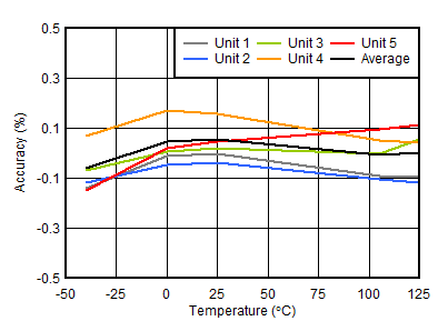
| TPS3852G33-Q1 |
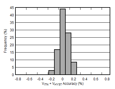
| Includes G and H versions with 3.3-V nominal monitored voltage, total units = 15,536 |
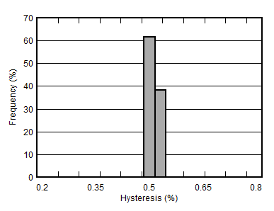
| Includes G and H versions with 3.3-V nominal monitored voltage, total units = 15,536 |
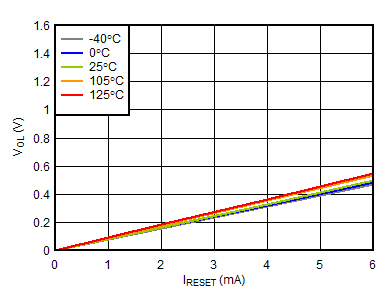
| VDD = 6.5 V |
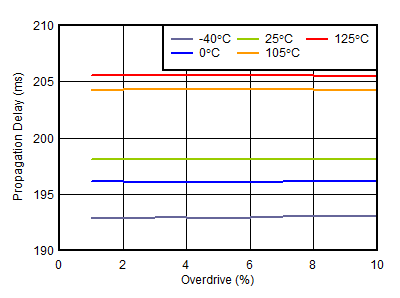
| TPS3852G33-Q1 exiting undervoltage |
