ZHCSFP5 November 2016 TPS3852
PRODUCTION DATA.
- 1 特性
- 2 应用
- 3 说明
- 4 修订历史记录
- 5 Pin Configuration and Functions
- 6 Specifications
- 7 Detailed Description
- 8 Application and Implementation
- 9 Power Supply Recommendations
- 10Layout
- 11器件和文档支持
- 12机械、封装和可订购信息
8 Application and Implementation
NOTE
Information in the following applications sections is not part of the TI component specification, and TI does not warrant its accuracy or completeness. TI’s customers are responsible for determining suitability of components for their purposes. Customers should validate and test their design implementation to confirm system functionality.
8.1 Application Information
8.1.1 CWD Functionality
The TPS3852 features three options for setting the watchdog window: connecting a capacitor to the CWD pin, connecting a pullup resistor to VDD, and leaving the CWD pin unconnected. Figure 18 shows a schematic drawing of all three options. If this pin is connected to VDD through a 10-kΩ pullup resistor or left unconnected (high impedance), then the factory-programmed watchdog timeouts are enabled; see the Timing Requirements table. Otherwise, the watchdog timeout can be adjusted by placing a capacitor from the CWD pin to ground.
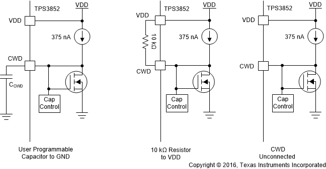 Figure 18. CWD Charging Circuit
8.1.1.1 Factory-Programmed Timing Options
If using the factory-programmed timing options (listed in Table 2), the CWD pin must either be unconnected or pulled up to VDD through a 10-kΩ pullup resistor. Using these options enables high-precision, 15% accurate watchdog timing.
Table 2. Factory-Programmed Watchdog Timing
| INPUT | WATCHDOG LOWER BOUNDARY (tWDL) | WATCHDOG UPPER BOUNDARY (tWDU) | UNIT | |||||
|---|---|---|---|---|---|---|---|---|
| CWD | SET1 | MIN | TYP | MAX | MIN | TYP | MAX | |
| NC | 0 | Watchdog disabled | Watchdog disabled | |||||
| 1 | 680 | 800 | 920 | 1360 | 1600 | 1840 | ms | |
| 10 kΩ to VDD | 0 | Watchdog disabled | Watchdog disabled | |||||
| 1 | 1.5 | 1.85 | 2.2 | 8.8 | 11.0 | 13.2 | ms | |
8.1.1.2 Adjustable Capacitor Timing
Adjustable capacitor timing is achievable by connecting a capacitor to the CWD pin. If a capacitor is connected to CWD, then a 375-nA current source charges CCWD until VCWD = 1.21 V. The TPS3852 determines the window watchdog upper boundary with the formula given in Equation 1, where CCWD is in microfarads (µF) and tWDU is in seconds.
The TPS3852 is limited to using CCWD capacitors between 100 pF and 1 µF. Note that Equation 1 is for ideal capacitors, capacitor tolerances cause the actual device timing to vary. For the most accurate timing, use ceramic capacitors with COG dielectric material. As shown in Table 4, when using the minimum capacitance of 100 pF, the watchdog upper boundary is 62.74 ms; whereas with a 1-µF capacitance, the watchdog upper boundary is 77.455 seconds. If a CCWD capacitor is used, Equation 1 can be used to set tWDU the window watchdog upper boundary. Table 3 shows how tWDU can be used to calculate tWDL.
Table 3. Programmable CWD Timing
| INPUT | WATCHDOG LOWER BOUNDARY (tWDL) | WATCHDOG UPPER BOUNDARY (tWDU) | UNIT | |||||
|---|---|---|---|---|---|---|---|---|
| CWD | SET1 | MIN | TYP | MAX | MIN | TYP | MAX | |
| CCWD | 0 | Watchdog disabled | Watchdog disabled | |||||
| 1 | tWDU(min) x 0.5 | tWDU x 0.5 | tWDU(max) x 0.5 | 0.85 x tWDU(typ) | tWDU(typ)(1) | 1.15 x tWDU(typ) | s | |
Table 4. tWDU Values for Common Ideal Capacitor Values
| CCWD | WATCHDOG UPPER BOUNDARY (tWDU) | UNIT | ||
|---|---|---|---|---|
| MIN(1) | TYP | MAX(1) | ||
| 100 pF | 53.32 | 62.74 | 72.15 | ms |
| 1 nF | 112.5 | 132.4 | 152.2 | ms |
| 10 nF | 704 | 829 | 953 | ms |
| 100 nF | 6625 | 7795 | 8964 | ms |
| 1 µF | 65836 | 77455 | 89073 | ms |
8.1.2 Overdrive Voltage
Forcing a RESET is dependent on two conditions: the amplitude VDD is beyond the trip point (ΔV1 and ΔV2), and the length of time that the voltage is beyond the trip point (t1 and t2). If the voltage is just under the trip point for a long period of time, RESET asserts and the output is pulled low. However, if VDD is just under the trip point for a few nanoseconds, RESET does not assert and the output remains high. The length of time required for RESET to assert can be changed by increasing the amount VDD goes under the trip point. If VDD is under the trip point by 10%, the amount of time required for the comparator to respond is much faster and causes RESET to assert much quicker than when barely under the trip point voltage. Equation 2 shows how to calculate the percentage overdrive.
In Equation 2, VITX corresponds to the threshold trip point. If VDD is exceeding the positive threshold, VITN + VHYST is used. VITN is used when VDD is falling below the negative threshold. In Figure 19, t1 and t2 correspond to the amount of time that VDD is over the threshold; the propagation delay versus overdrive for VITN and VITN + VHYST is illustrated in Figure 13 and Figure 14, respectively.
The TPS3852 is relatively immune to short positive and negative transients on VDD because of the overdrive voltage.
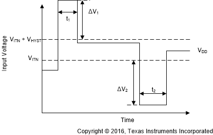 Figure 19. Overdrive Voltage
8.2 Typical Application
A typical application for the TPS3852 is shown in Figure 20. The TPS3852G33 is used to monitor the 3.3-V, VCORE rail powering the microcontroller.
 Figure 20. Monitoring Supply Voltage and Watchdog Supervision of a Microcontroller
8.2.1 Design Requirements
| Parameter | Design Requirement | Design Result |
|---|---|---|
| Watchdog Disable For Initialization Period | Watchdog must remain disabled for 7 seconds until logic enables the watchdog timer | 7.21 seconds (typ) |
| Output Logic Voltage | 3.3V CMOS | 3.3V CMOS |
| Monitored Rail | 3.3 V with a 5% threshold | Worst Case VITN = 3.142 V (- 4.7% threshold) |
| Watchdog Window | 250 ms, maximum | tWDL(max) = 135 ms, tWDU(min) = 181 ms |
| Maximum Device Current Consumption | 50 uA | 52 uA (worst case) when RESET or WDO is asserted(1) |
8.2.2 Detailed Design Procedure
8.2.2.1 Monitoring the 3.3V Rail
This application calls for very tight monitoring of the rail with only 5% of variation allowed on the rail. To ensure this requirement is met, the TPS3852G33 was chosen for its -4% threshold. To calculate the worst-case for VITN, the accuracy must also be taken into account. The worst-case for VITN can be calculated by Equation 3:
8.2.2.2 Calculating RESET and WDO Pullup Resistor
The TPS3852 uses an open-drain configuration for the RESET circuit, as shown in Figure 21. When the FET is off, the resistor pulls the drain of the transistor to VDD and when the FET is turned on, the FET attempts to pull the drain to ground, thus creating an effective resistor divider. The resistors in this divider must be chosen to ensure that VOL is below the maximum value. To choose the proper pullup resistor, there are three key specifications to keep in mind: the pullup voltage (VPU), the recommended maximum RESET pin current (IRESET), and VOL. The maximum VOL is 0.4 V, meaning that the effective resistor divider created must be able to bring the voltage on the reset pin below 0.4 V with IRESET kept below 10 mA. For this example, with a VPU of 3.3 V, a resistor must be chosen to keep IRESET below 50 μA because this value is the maximum consumption current allowed. To ensure this specification is met, a pullup resistor value of 100 kΩ was selected, which sinks a maximum of 33 μA when RESET or WDO is asserted. As illustrated in Figure 11, when the RESET current is at 33 μA and the low-level output voltage is approximately zero.
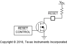 Figure 21. RESET Open-Drain Configuration
8.2.2.3 Setting the Window Watchdog
As illustrated in Figure 18, there are three options for setting the window watchdog. The design specifications in this application require the programmable timing option (external capacitor connected to CWD). When a capacitor is connected to the CWD pin, the window is governed by Equation 4. Equation 4 is only valid for ideal capacitors, any temperature or voltage derating must be accounted for separately.

The nearest standard capacitor value to 2.5 nF is 2.2 nF. Selecting 2.2 nF for the CCWD capacitor gives the following minimum and maximum timing parameters:


Capacitor tolerance also influence tWDU(MIN) and tWDL(MAX). Select a ceramic COG dielectric capacitor for high accuracy. For 2.2 nF, COG capacitors are readily available with a 5% tolerance, which results in a 5% decrease in tWDU(MIN) and a 5% increase in tWDL(MAX), giving 181 ms and 135 ms, respectively. A falling edge must be issued within this window.
8.2.2.4 Watchdog Disabled During Initialization Period
The watchdog is often needed to be disabled during startup to allow for an initialization period. When the initialization period is over, the watchdog timer is turned back on to allow the microcontroller to be monitored by the TPS3852. To achieve this setup SET1 must start at GND. In this design, SET1 is controlled by a TPS3890 supervisor. In this application, the TPS3890 was chosen to monitor VDD as well, which means that RESET on the TPS3890 stays low until VDD rises above VITN. When VDD comes up, the delay time can be adjusted through the CT capacitor on the TPS3890. With this approach, the RESET delay can be adjusted from a minimum of 25 µs to a maximum of 30 seconds. For this design, a minimum delay of 7 seconds is needed until the watchdog timer is enabled. The CT capacitor calculation (see the TPS3890 data sheet) yields an ideal capacitance of 6.59 µF, giving a closest standard ceramic capacitor value of 6.8 µF. When connecting a 6.8-µF capacitor from CT to GND, the typical delay time is 7.21 seconds. Figure 22 illustrates the typical startup waveform for this circuit when the watchdog input is off. Figure 22 illustrates that when the watchdog is disabled, the WDO output remains high. See the TPS3890 data sheet for detailed information on the TPS3890.
8.2.3 Glitch Immunity
Figure 25 shows the high to low glitch immunity for the TPS3852G33 with a 7% overdrive with VDD starting at 3.3 V. This curve shows that VDD can go below the threshold for 5.2 µs without RESET asserting.
8.2.4 Application Curves
Unless otherwise stated, application curves were taken at TA = 25°C.
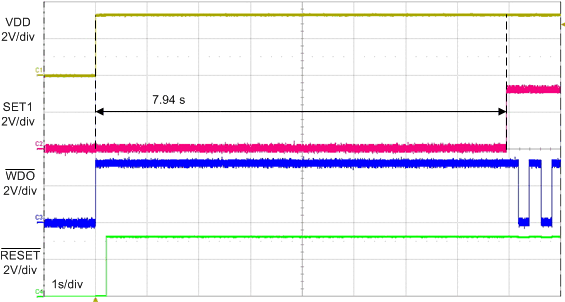 Figure 22. Startup Without a WDI Signal
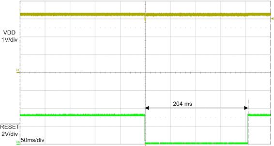 Figure 24. Typical RESET Delay
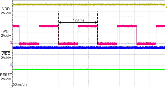 Figure 23. Typical WDI Signal
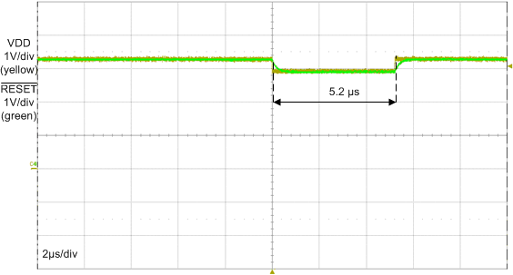 Figure 25. High to Low Glitch Immunity