SBVS149B September 2010 – January 2016 TPS386000-Q1
PRODUCTION DATA.
- 1 Features
- 2 Applications
- 3 Description
- 4 Revision History
- 5 Pin Configuration and Functions
- 6 Specifications
- 7 Parametric Measurement information
- 8 Detailed Description
- 9 Application and Implementation
- 10Power Supply Recommendations
- 11Layout
- 12Device and Documentation Support
- 13Mechanical, Packaging, and Orderable Information
8 Detailed Description
8.1 Overview
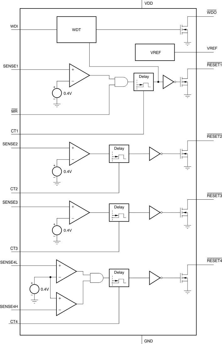
The TPS386000-Q1 multi-channel supervisory device family combines four complete SVS function sets into one IC. The design of each SVS channel is based on the single-channel supervisory device series, TPS3808. The TPS386000-Q1 is designed to assert RESETn or RESETn signals, as shown in Table 1, Table 2, Table 3, and Table 4. The RESETn or RESETn outputs remain asserted during a user-configurable delay time after the event of reset release (see the Reset Delay Time section).
8.2 Functional Block Diagram
 Figure 28. TPS386000-Q1
8.3 Feature Description
8.3.1 Voltage Monitoring
Each SENSEm (m = 1, 2, 3, 4L) pin can be set to any voltage threshold above 0.4 V using an external resistor divider. The SENSE4H pin can be used for any overvoltage detection greater than 0.4 V, or for negative voltage detection using an external resistor divider (see the section). A broad range of voltage threshold and reset delay time adjustments can be supported, allowing these devices to be used in a wide array of applications.
8.3.2 RESET Output
In a typical TPS386000-Q1 application, RESETn or RESETn outputs are connected to the reset input of a processor (DSP, CPU, FPGA, ASIC, etc.), or connected to the enable input of a voltage regulator (DC-DC, LDO, etc.)
The TPS386000-Q1 provides open-drain reset outputs. Pullup resistors must be used to hold these lines high when RESETn is not asserted, or when RESETn is asserted. By connecting pullup resistors to the proper voltage rails (up to 6.5 V), RESETn or RESETn output nodes can be connected to the other devices at the correct interface voltage levels. The pullup resistor should be no smaller than 10 kΩ because of the safe operation of the output transistors. By using wired-OR logic, any combination of RESETn can be merged into one logic signal.
All RESETn or RESETn connections must be compatible with the VDD logic level.
The RESETn or RESETn outputs are defined for VDD voltage higher than 0.9 V. To ensure that the target processor(s) are properly reset, the VDD supply input should be fed by the available power rail as early as possible in application circuits. Table 1, Table 2, Table 3, and Table 4 are truth tables that describe how the outputs are asserted or released. Figure 1, Figure 2, Figure 3, and Figure 4 show the SVS-n timing diagrams. When the condition(s) are met, the device changes the state of SVS-n from asserted to released after a user-configurable delay time. However, the transitions from released-state to asserted-state are performed almost immediately with minimal propagation delay. Figure 3 describes relationship between threshold voltages (VIT– and VHYS–) and SENSEm voltage; and all SVS-1, SVS-2, SVS-3, and SVS-4 have the same behavior of Figure 3.
8.3.3 Manual Reset
The manual reset (MR) input allows external logic signal from other processors, logic circuits, and/or discrete sensors to initiate a device reset. Because MR is connected to SVS-1, the RESET1 or RESET1 pin is intended to be connected to processor(s) as a primary reset source. A logic low at MR causes RESET1 or RESET1 to assert. After MR returns to a logic high and SENSE1 is above its reset threshold, RESET1 or RESET1 is released after the user-configured reset delay time. Note that unlike the TPS3808 series, the TPS386000-Q1 does not integrate an internal pullup resistor between MR and VDD.
To control the MR function from more than one logic signal, the logic signals can be combined by wired-OR into the MR pin using multiple NMOS transistors and one pullup resistor.
8.3.4 Watchdog Timer
The TPS386000-Q1 provides a watchdog timer with a dedicated watchdog error output, WDO or WDO. The WDO or WDO output enables application board designers to easily detect and resolve the hang-up status of a processor. As with MR, the watchdog timer function of the device is also tied to SVS-1. Figure 5 shows the timing diagram of the WDT function. Once RESET1 or RESET1 is released, the internal watchdog timer starts its countdown. Inputting a logic level transition at WDI resets the internal timer count and the timer restarts the countdown. If the TPS386000-Q1 fails to receive any WDI rising or falling edge within the WDT period, the WDT times out and asserts WDO or WDO. After WDO or WDO is asserted, the device holds the status with the internal latch circuit. To clear this timeout status, a reset assertion of RESET1 or RESET is required. That is, a negative pulse to MR, a SENSE1 voltage less than VIT–, or a VDD power-down is required.
To reset the processor by WDT timeout, WDO can be combined with RESET1 by using the wired-OR with the TPS386000-Q1 option.
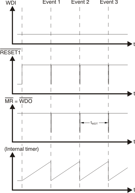
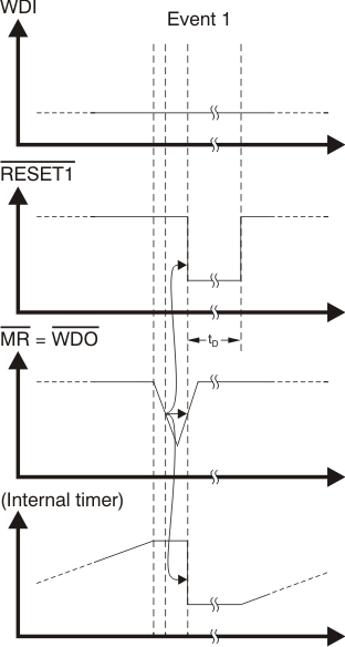
For legacy applications where the watchdog timer timeout causes RESET1 to assert, connect WDO to MR; see Figure 31 for the connections and see Figure 29 and Figure 30 for the timing diagram. This legacy support configuration is available with the TPS386000-Q1.
8.3.5 Immunity to SENSEn Voltage Transients
The TPS386000-Q1 is relatively immune to short negative transients on the SENSEn pin. Sensitivity to transients depends on threshold overdrive, as shown in the typical performance graph TPS386000-Q1 SENSEn Minimum Pulse Width vs SENSEn Threshold Overdrive Voltage (Figure 12).
 Figure 29. Legacy WDT Configuration Timing Diagram
 Figure 30. Enlarged View of Event 1 from Figure 29
8.4 Device Functional Modes
8.4.1 Overview
The TPS386000-Q1 multi-channel supervisory device family combines four complete SVS function sets into one IC. The design of each SVS channel is based on the single-channel supervisory device series, TPS3808. The TPS386000-Q1 is designed to assert RESETn or RESETn signals, as shown in Table 1, Table 2, Table 3, and Table 4. The RESETn or RESETn outputs remain asserted during a user-configurable delay time after the event of reset release (see the Reset Delay Time section).
Table 1. SVS-1 Truth Table
| CONDITION | OUTPUT | STATUS | |
|---|---|---|---|
| TPS386000-Q1 | |||
| MR = Low | SENSE1 < VIT– | RESET1 = Low | Reset asserted |
| MR = Low | SENSE1 > VIT– | RESET1 = Low | Reset asserted |
| MR = High | SENSE1 < VIT– | RESET1 = Low | Reset asserted |
| MR = High | SENSE1 > VIT– | RESET1 = High | Reset released after delay |
Table 2. SVS-2 Truth Table
| CONDITION | OUTPUT | STATUS |
|---|---|---|
| TPS386000-Q1 | ||
| SENSE2 < VIT– | RESET2 = Low | Reset asserted |
| SENSE2 > VIT– | RESET2 = High | Reset released after delay |
Table 3. SVS-3 Truth Table
| CONDITION | OUTPUT | STATUS |
|---|---|---|
| TPS386000-Q1 | ||
| SENSE3 < VIT– | RESET3 = Low | Reset asserted |
| SENSE3 > VIT– | RESET3 = High | Reset released after delay |
Table 4. SVS-4 Truth Table
| CONDITION | OUTPUT | STATUS | |
|---|---|---|---|
| TPS386000-Q1 | |||
| SENSE4L < VIT– | SENSE4H > VIT+ | RESET4 = Low | Reset asserted |
| SENSE4L < VIT– | SENSE4H < VIT+ | RESET4 = Low | Reset asserted |
| SENSE4L > VIT– | SENSE4H > VIT+ | RESET4 = Low | Reset asserted |
| SENSE4L > VIT– | SENSE4H < VIT+ | RESET4 = High | Reset released after delay |
Table 5. Watchdog Timer (WDT) Truth Table
| CONDITION | OUTPUT | STATUS | |||
|---|---|---|---|---|---|
| WDO | WDO | RESET1 OR RESET1 | WDI PULSE INPUT | TPS386000-Q1 | |
| Low | High | Asserted | Toggling | WDO = low | Remains in WDT timeout |
| Low | High | Asserted | 610 ms after last WDI↑ or WDI↓ | WDO = low | Remains in WDT timeout |
| Low | High | Released | Toggling | WDO = low | Remains in WDT timeout |
| Low | High | Released | 610 ms after last WDI↑ or WDI↓ | WDO = low | Remains in WDT timeout |
| High | Low | Asserted | Toggling | WDO = high | Normal operation |
| High | Low | Asserted | 610 ms after last WDI↑ or WDI↓ | WDO = high | Normal operation |
| High | Low | Released | Toggling | WDO = high | Normal operation |
| High | Low | Released | 610 ms after last WDI↑ or WDI↓ | WDO = low | Enters WDT timeout |