SLVSA75A July 2010 – August 2015 TPS386596
PRODUCTION DATA.
- 1 Features
- 2 Applications
- 3 Description
- 4 Revision History
- 5 Pin Configuration and Functions
- 6 Specifications
- 7 Parameter Measurement Information
- 8 Detailed Description
- 9 Application and Implementation
- 10Power Supply Recommendations
- 11Layout
- 12Device and Documentation Support
- 13Mechanical, Packaging, and Orderable Information
9 Application and Implementation
NOTE
Information in the following applications sections is not part of the TI component specification, and TI does not warrant its accuracy or completeness. TI’s customers are responsible for determining suitability of components for their purposes. Customers should validate and test their design implementation to confirm system functionality.
9.1 Application Information
9.1.1 Undervoltage Detection
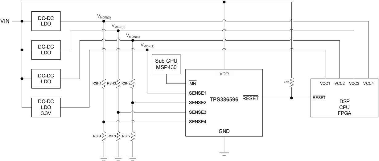
The SENSEn inputs provide terminals at which the system voltages can be monitored. If the voltage at any one of the SENSEn pins drops the respective VITn, then the RESET output is asserted. The comparators have a built-in hysteresis to ensure smooth RESET transitions.
It is good analog design practice to use a 1-nF to 10-nF bypass capacitor at the SENSEn input to ground, to reduce sensitivity to transients, layout parasitics, and interference between power rails monitored by this device.
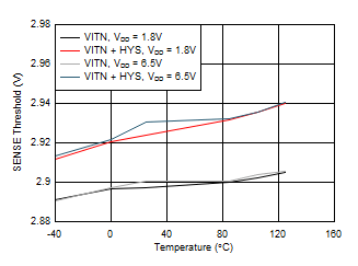
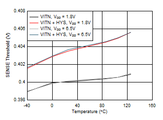
A typical connection of resistor dividers is show in Figure 14. SENSE1 is used to monitor a 3.3-V nominal power-supply voltage with a trip point equal to 2.90 V, and the remaining SENSEn (n = 2, 3, 4) inputs can be used to monitor voltage rails down to 0.4 V. Threshold voltages can be calculated using the following equations.
9.2 Typical Application
Figure 14 shows a typical application for the TPS386956.
9.2.1 Design Requirements
This design is intended to monitor the voltage rails for an FPGA. Table 2 summarizes the design requirements.
Table 2. Design Requirements
| PARAMETER | DESIGN REQUIREMENT |
|---|---|
| VDD | 5 V |
| VMON(1) | 3.3 V –10% |
| VMON(2) | 1.5 V –5% |
| VMON(3) | 1.2 V –5% |
| VMON(4) | 1 V –5% |
9.2.2 Detailed Design Procedure
Select the pullup resistors to be 100 kΩ to ensure that VOL ≤ 0.4 V.
Select RSnL = 10 kΩ for all channels to ensure DC accuracy.
Use Equation 1 through Equation 3 to determine the values of RSnH and RS4M. Using standard 1% resistors, Table 3 shows the results:
Table 3. Design Results
| RESISTOR | VALUE (kΩ) |
|---|---|
| RS1H | 32.4 |
| RS2H | 25.5 |
| RS3H | 18.7 |
| RS4H | 14.3 |
| RS4M | 1 |
9.2.3 Application Curves
