ZHCSG28B March 2017 – February 2018 TPS3890-Q1
PRODUCTION DATA.
- 1 特性
- 2 应用
- 3 说明
- 4 修订历史记录
- 5 Device Comparison Table
- 6 Pin Configuration and Functions
- 7 Specifications
- 8 Detailed Description
- 9 Application and Implementation
- 10Power Supply Recommendations
- 11Layout
- 12器件和文档支持
- 13机械、封装和可订购信息
8.3.4 SENSE Input
The SENSE input can vary from ground to 5.5 V (7.0 V, absolute maximum), regardless of the device supply voltage used. The SENSE pin is used to monitor the critical voltage rail. If the voltage on this pin drops below VITN, then RESET is asserted. When the voltage on the SENSE pin exceeds the positive threshold voltage, RESET deasserts after the user-defined RESET delay time.
The internal comparator has built-in hysteresis to ensure well-defined RESET assertions and deassertions even when there are small changes on the voltage rail being monitored.
The TPS3890-Q1 device is relatively immune to short transients on the SENSE pin. Glitch immunity is dependent on threshold overdrive, as illustrated in Figure 19 for VITN and Figure 18 for VITP. Although not required in most cases, for noisy applications good analog design practice is to place a 1-nF to 10-nF bypass capacitor at the SENSE input to reduce sensitivity to transient voltages on the monitored signal.
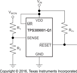
The adjustable version (TPS389001-Q1) can be used to monitor any voltage rail down to 1.15 V using the circuit shown in Figure 24.
 Figure 24. Using the TPS389001-Q1 to Monitor a User-Defined Threshold Voltage
The target threshold voltage for the monitored supply (VITx(MON)) and the resistor divider values can be calculated by using Equation 2 and Equation 3, respectively:
Equation 3 can be used to calculate either the negative threshold or the positive threshold by replacing VITx with either VITN or VITP, respectively.
Resistors with high values minimize current consumption; however, the input bias current of the device degrades accuracy if the current through the resistors is too low. Therefore, choosing an RTOTAL value so that the current through the resistor divider is at least 100 times larger than the SENSE input current is simplest. See the Optimizing Resistor Dividers at a Comparator Input application report for more details on sizing input resistors.