ZHCSF70A March 2016 – May 2016 TPS3890
PRODUCTION DATA.
- 1 特性
- 2 应用
- 3 说明
- 4 修订历史记录
- 5 Device Comparison Table
- 6 Pin Configuration and Functions
- 7 Specifications
- 8 Detailed Description
- 9 Application and Implementation
- 10Power Supply Recommendations
- 11Layout
- 12器件和文档支持
- 13机械、封装和可订购信息
7 Specifications
7.1 Absolute Maximum Ratings
over operating junction temperature range (unless otherwise noted)(1)| MIN | MAX | UNIT | ||
|---|---|---|---|---|
| Voltage | VDD | –0.3 | 7 | V |
| SENSE | –0.3 | 7 | ||
| RESET | –0.3 | 7 | ||
| MR | –0.3 | 7 | ||
| VCT | –0.3 | 7 | ||
| Current | RESET | –20 | 20 | mA |
| Temperature | Operating junction temperature, TJ | –40 | 125 | °C |
| Storage temperature, Tstg | –65 | 150 | ||
(1) Stresses beyond those listed under Absolute Maximum Ratings may cause permanent damage to the device. These are stress ratings only, which do not imply functional operation of the device at these or any other conditions beyond those indicated under Recommended Operating Conditions. Exposure to absolute-maximum-rated conditions for extended periods may affect device reliability.
7.2 ESD Ratings
| VALUE | UNIT | |||
|---|---|---|---|---|
| V(ESD) | Electrostatic discharge | Human-body model (HBM), per ANSI/ESDA/JEDEC JS-001(1) | ±1000 | V |
| Charged-device model (CDM), per JEDEC specification JESD22-C101(2) | ±750 | |||
(1) JEDEC document JEP155 states that 500-V HBM allows safe manufacturing with a standard ESD control process. Manufacturing with less than 500-V HBM is possible with the necessary precautions.
(2) JEDEC document JEP157 states that 250-V CDM allows safe manufacturing with a standard ESD control process. Manufacturing with less than 250-V CDM is possible with the necessary precautions.
7.3 Recommended Operating Conditions
over operating free-air temperature range (unless otherwise noted)| MIN | NOM | MAX | UNIT | ||
|---|---|---|---|---|---|
| VDD | Power-supply voltage | 1.5 | 5.5 | V | |
| VSENSE | SENSE voltage | 0 | 5.5 | V | |
| VRESET | RESET pin voltage | 0 | 5.5 | V | |
| IRESET | RESET pin current | –5 | 5 | mA | |
| CIN | Input capacitor, VDD pin | 0 | 0.1 | µF | |
| CCT | Reset timeout capacitor, CT pin | 0 | 22 | µF | |
| RPU | Pullup resistor, RESET pin | 1 | 1000 | kΩ | |
| TJ | Junction temperature (free-air temperature) | –40 | 25 | 125 | ℃ |
7.4 Thermal Information
| THERMAL METRIC(1) | TPS3890 | UNIT | |
|---|---|---|---|
| DSE (WSON) | |||
| 6 PINS | |||
| RθJA | Junction-to-ambient thermal resistance | 321.3 | °C/W |
| RθJC(top) | Junction-to-case (top) thermal resistance | 207.9 | °C/W |
| RθJB | Junction-to-board thermal resistance | 281.5 | °C/W |
| ψJT | Junction-to-top characterization parameter | 42.4 | °C/W |
| ψJB | Junction-to-board characterization parameter | 284.8 | °C/W |
| RθJC(bot) | Junction-to-case (bottom) thermal resistance | 142.3 | °C/W |
(1) For more information about traditional and new thermal metrics, see the Semiconductor and IC Package Thermal Metrics application report, SPRA953.
7.5 Electrical Characteristics
over the operating junction temperature range of –40°C to +125°C, 1.5 V ≤ VDD ≤ 5.5 V, and MR = VDD (unless otherwise noted); typical values are at VDD = 5.5 V and TJ = 25°C| PARAMETER | TEST CONDITIONS | MIN | TYP | MAX | UNIT | |
|---|---|---|---|---|---|---|
| VDD | Input supply voltage | 1.5 | 5.5 | V | ||
| VPOR | Power-on reset voltage | VOL(max) = 0.2 V, IRESET = 15 µA | 0.8 | V | ||
| IDD | Supply current (into VDD pin) | VDD = 3.3 V, IRESET = 0 mA, –40°C < TJ < 85°C |
2.09 | 3.72 | µA | |
| VDD = 3.3 V, IRESET = 0 mA, –40°C < TJ < 105°C |
4.5 | |||||
| VDD= 3.3 V, IRESET = 0 mA | 5.8 | |||||
| VDD = 5.5 V, IRESET = 0 mA, –40°C < TJ < 85°C |
2.29 | 4 | ||||
| VDD = 5.5 V, IRESET = 0 mA, –40°C < TJ < 105°C |
5.2 | |||||
| VDD = 5.5 V, IRESET = 0 mA | 6.5 | |||||
| VITN, VITP | SENSE input threshold voltage accuracy | –1% | ±0.5% | 1% | ||
| VHYST | Hysteresis(1) | 0.325% | 0.575% | 0.825% | ||
| ISENSE | Input current | VSENSE = 5 V | 8 | µA | ||
| VSENSE = 5 V, TPS389001, TPS389012 | 10 | 100 | nA | |||
| ICT | CT pin charge current | 0.90 | 1.15 | 1.35 | µA | |
| VCT | CT pin comparator threshold voltage | 1.17 | 1.23 | 1.29 | V | |
| RCT | CT pin pulldown resistance | When RESET is deasserted | 200 | Ω | ||
| VIL | Low-level input voltage (MR pin) | 0.25 × VDD | V | |||
| VIH | High-level output voltage | 0.7 x VDD | V | |||
| VOL | Low-level output voltage | VDD ≥ 1.5 V, IRESET = 0.4 mA | 0.25 | V | ||
| VDD ≥ 2.7 V, IRESET = 2 mA | 0.25 | |||||
| VDD ≥ 4.5 V, IRESET = 3 mA | 0.3 | |||||
| ILKG(OD) | Open-drain output leakage | High impedance, VSENSE = VRESET = 5.5 V |
250 | nA | ||
(1) VHYST = [(VITP – VITN) / VITN] × 100%.
7.6 Timing Requirements
over the operating junction temperature range of –40°C to +125°C, 1.5 V ≤ VDD ≤ 5.5 V, MR = VDD, and 5% input overdrive(1) (unless otherwise noted); typical values are at VDD = 5.5 V and TJ = 25°C| MIN | NOM | MAX | UNIT | |||
|---|---|---|---|---|---|---|
| tPD(f) | SENSE (falling) to RESET propagation delay | CT = open, VDD = 3.3 V | 18 | µs | ||
| CT = open, VDD = 5.5 V | 8 | |||||
| tPD(r) | SENSE (rising) to RESET propagation delay | CT = open, VDD = 3.3 V | 25 | µs | ||
| tGI(SENSE) | SENSE pin glitch immunity | VDD = 5.5 V | 9 | µs | ||
| tGI(MR) | MR pin glitch immunity | VDD = 5.5 V | 100 | ns | ||
| tMRW | MR pin pulse duration to assert RESET | 1 | µs | |||
| td(MR) | MR pin low to out delay | 250 | ns | |||
| tSTRT | Startup delay | 325 | µs | |||
(1) Overdrive = | (VIN / VTHRESH – 1) × 100% |.
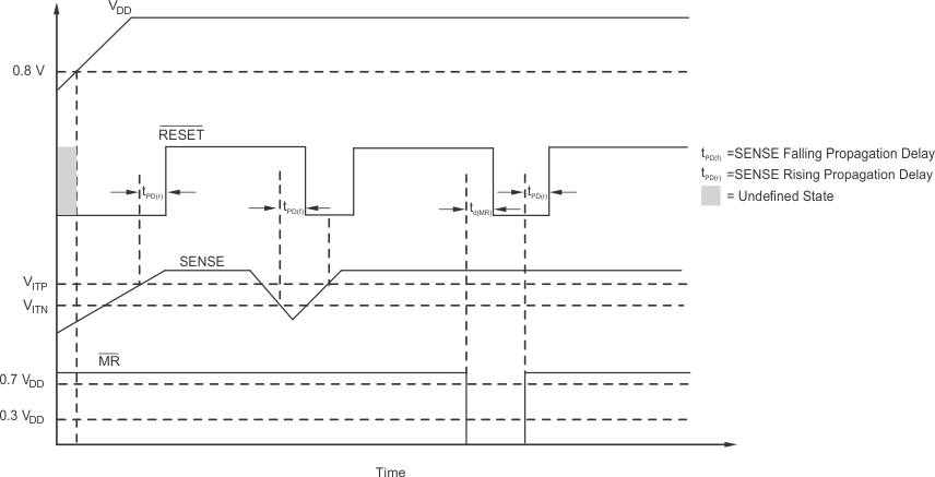 Figure 1. Timing Diagram
7.7 Typical Characteristics
over the operating junction temperature range of –40°C to +125°C, 1.5 V ≤ VDD ≤ 5.5 V, and MR = VDD (unless otherwise noted)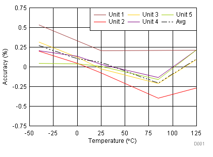
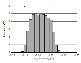
| Tested at VDD = 1.5 V and VDD = 5.5 V, total tests = 136,348 |
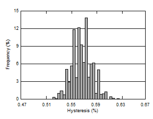
i.
Figure 6. Hysteresis Histogram
| Tested at VDD = 1.5 V and VDD = 5.5 V, total tests = 136,348 |
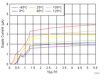
| MR = VDD |
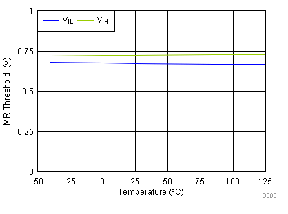
| VDD = 1.5 V |
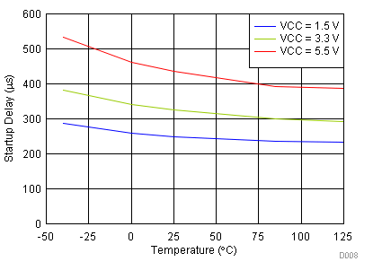
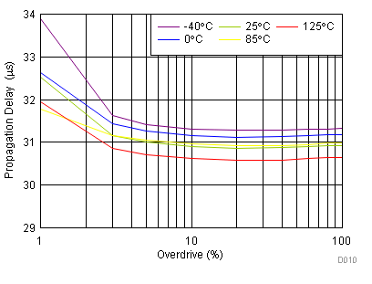
| VDD = 1.5 V |
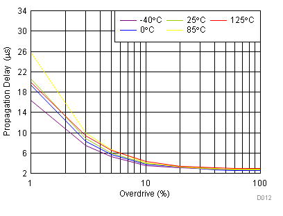
| VDD = 1.5 V |
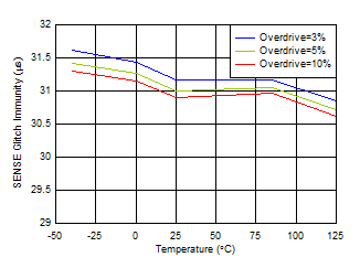
| VDD = 1.5 V |
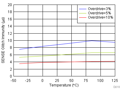
| VDD = 1.5 V |

| VDD = 1.5 V |
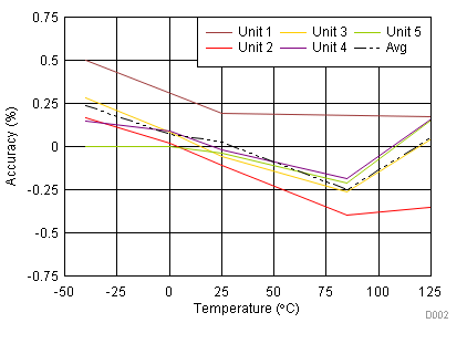
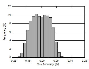
| Tested at VDD = 1.5 V and VDD = 5.5 V, total tests = 136,348 |
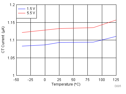
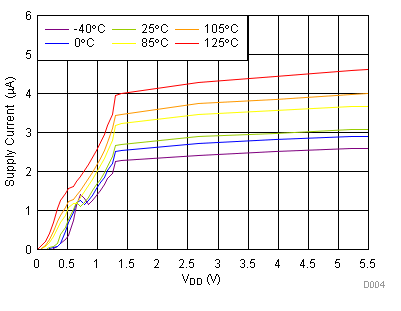
| MR = 0 V |
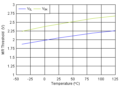
| VDD = 5.5 V |
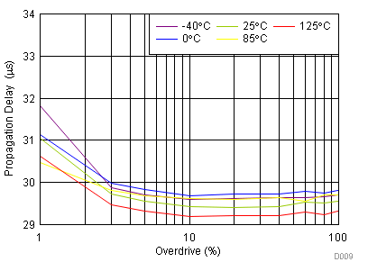
| VDD = 5.5 V |
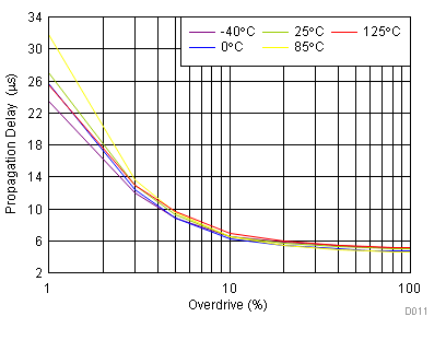
| VDD = 5.5 V |
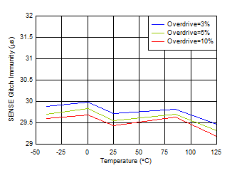
| VDD = 5.5 V |
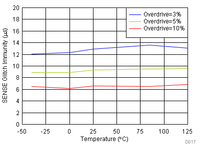
| VDD = 5.5 V |
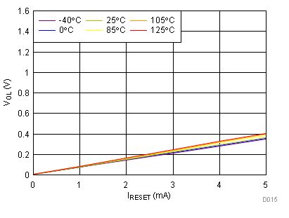
| VDD = 5.5 V |