ZHCS329B July 2011 – April 2015
PRODUCTION DATA.
- 1 特性
- 2 应用
- 3 说明
- 4 修订历史记录
- 5 Device Comparison Table
- 6 Pin Configuration and Functions
- 7 Specifications
- 8 Detailed Description
- 9 Applications and Implementation
- 10Power Supply Recommendations
- 11Layout
- 12器件和文档支持
- 13机械、封装和可订购信息
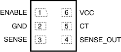
6 Pin Configuration and Functions
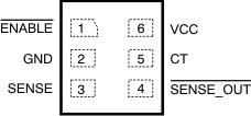
DRY Package: TPS3896, TPS3898
6-Pin USON
Top View

Pin Functions
| PIN | I/O | DESCRIPTION | ||
|---|---|---|---|---|
| NAME | USON | |||
| TPS3895/ TPS3897 |
TPS3896/ TPS3898 |
|||
| CT | 5 | 5 | I | Capacitor-adjustable delay. The CT pin offers a user-adjustable delay time. Connecting this pin to a ground referenced capacitor sets the delay time for SENSE rising above 0.5 V to SENSE_OUT asserting (or ENABLE asserting to SENSE_OUT asserting for A version devices). tpd(r) (s) = [CCT (µF) × 4] + 40 µs |
| ENABLE | 1 | — | I | Active high input. Driving ENABLE low immediately makes SENSE_OUT go low, independent of V(SENSE). With V(SENSE) already above VIT+, drive ENABLE high to make SENSE_OUT go high after the capacitor-adjustable delay time (A version) or 0.2 µs (P version). |
| ENABLE | — | 1 | I | Active low input. Driving ENABLE high immediately makes SENSE_OUT go high, independent of V(SENSE). With V(SENSE) already above VIT+, drive ENABLE low to make SENSE_OUT go low after the capacitor-adjustable delay time (A version) or 0.2 µs (P version). |
| GND | 2 | 2 | — | Ground |
| SENSE | 3 | 3 | I | This pin is connected to the voltage that is monitored with the use of an external resistor. The output asserts after the capacitor-adjustable delay time when V(SENSE) rises above 0.5 V and ENABLE is asserted. The output deasserts after a minimal propagation delay (16 µs) when V(SENSE) falls below VIT+ – Vhys. |
| SENSE_OUT | 4 | — | O | SENSE_OUT is an open-drain and push-pull output that is immediately driven low after V(SENSE) falls below (VIT+ – Vhys) or the ENABLE input is low. SENSE_OUT goes high after the capacitor-adjustable delay time when V(SENSE) is greater than VIT+ and the ENABLE pin is high. Open-drain devices (TPS3897/8) can be pulled up to 18 V independent of VCC; pullup resistors are required for these devices. |
| SENSE_OUT | — | 4 | O | SENSE_OUT is an open-drain and push-pull output that is immediately driven high after V(SENSE) falls below (VIT+ – Vhys) or the ENABLE input is high. SENSE_OUT goes low after the capacitor-adjustable delay time when V(SENSE) is greater than VIT+ and the ENABLE pin is low. Open-drain devices (TPS3897/8) can be pulled up to 18 V independent of VCC; pullup resistors are required for these devices. |
| VCC | 6 | 6 | I | Supply voltage input. Connect a 1.7-V to 6.5-V supply to VCC to power the device. It is good analog design practice to place a 0.1-µF ceramic capacitor close to this pin. |
