ZHCSNL0B April 2021 – January 2024 TPS3899-Q1
PRODUCTION DATA
- 1
- 1 特性
- 2 应用
- 3 说明
- 4 Device Nomenclature
- 5 Pin Configuration and Functions
- 6 Specifications
- 7 Detailed Description
- 8 Application and Implementation
- 9 Device and Documentation Support
- 10Revision History
- 11Mechanical, Packaging, and Orderable Information
5 Pin Configuration and Functions
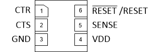
 Figure 5-1 DSE Package
6-Pin WSON
TPS3899-Q1 (Top View)
Table 5-1 Pin Functions
| PIN | I/O | DESCRIPTION | |
|---|---|---|---|
| NO. | NAME | ||
| 1 | CTR | — | Capacitor programmable reset delay: The CTR pin offers a user-adjustable delay time when returning from reset condition. Connecting this pin to a ground-referenced capacitor sets the RESET/RESET delay time to deassert. |
| 2 | CTS | — | Capacitor programmable sense delay: The CTS pin offers a user-adjustable delay time when asserting reset condition. Connecting this pin to a ground-referenced capacitor sets the RESET/RESET delay time to assert. |
| 3 | GND | — | Ground |
| 4 | VDD | I | Supply voltage pin: Good analog design practice is to place a 0.1µF decoupling capacitor close to this pin. |
| 5 | SENSE | I | This pin is connected to the voltage that
will be monitored for fixed variants or to a resistor divider for
the adjustable variant. When the voltage on the SENSE pin
transitions below the negative threshold voltage VIT-,
RESET/RESET asserts to active logic after
the sense delay set by CTS. When the voltage on the SENSE pin
transitions above the positive threshold voltage VIT- +
VHYS, RESET/RESET releases to
inactive logic (deasserts) after the reset delay set by CTR. For
noisy applications, placing a 10nF to 100nF ceramic capacitor close to this pin may be needed for optimum performance. |
| 6 | RESET | O | RESET active-low output that asserts to a logic low state after CTS delay when the monitored voltage on the SENSE pin is lower than the negative threshold voltage VIT-. RESET remains logic low (asserted) until the SENSE input rises above VIT- + VHYS and the CTR reset delay expires. |
| 6 | RESET | O | RESET active-high output that asserts to a logic high state after CTS delay when the monitored voltage on the SENSE pin is lower than the negative threshold voltage VIT-. RESET remains logic high (asserted) until the SENSE input rises above VIT- + VHYS and the CTR reset delay expires. |