ZHCSAK8J December 2003 – June 2022 TPS40054 , TPS40055 , TPS40057
PRODUCTION DATA
- 1 特性
- 2 应用
- 3 说明
- 4 Revision History
- 5 Pin Configuration and Functions
- 6 Specifications
-
7 Detailed Description
- 7.1 Overview
- 7.2 Functional Block Diagram
- 7.3
Feature Description
- 7.3.1 Setting the Switching Frequency (Programming the Clock Oscillator)
- 7.3.2 Programming The Ramp Generator Circuit
- 7.3.3 UVLO Operation
- 7.3.4 BP5 and BP10 Internal Voltage Regulators
- 7.3.5 Programming Soft Start
- 7.3.6 Programming Current Limit
- 7.3.7 Synchronizing to an External Supply
- 7.3.8 Loop Compensation
- 7.4 Device Functional Modes
-
8 Application and Implementation
- 8.1 Application Information
- 8.2
Typical Application
- 8.2.1 Design Requirements
- 8.2.2
Detailed Design Procedure
- 8.2.2.1 Calculate Maximum and Minimum Duty Cycles
- 8.2.2.2 Select Switching Frequency
- 8.2.2.3 Select ΔI
- 8.2.2.4 Calculate the High-Side MOSFET Power Losses
- 8.2.2.5 Calculate Synchronous Rectifier Losses
- 8.2.2.6 Calculate the Inductor Value
- 8.2.2.7 Set the Switching Frequency
- 8.2.2.8 Program the Ramp Generator Circuit
- 8.2.2.9 Calculate the Output Capacitance (CO)
- 8.2.2.10 Calculate the Soft-Start Capacitor (CSS/SD)
- 8.2.2.11 Calculate the Current Limit Resistor (RILIM)
- 8.2.2.12 Calculate Loop Compensation Values
- 8.2.2.13 Calculate the Boost and BP10V Bypass Capacitance
- 8.2.3 Application Curves
- 9 Power Supply Recommendations
- 10Layout
- 11Device and Documentation Support
- 12Mechanical, Packaging, and Orderable Information
8.1.7 TPS4005x Power Dissipation
The power dissipation in the TPS4005x is largely dependent on the MOSFET driver currents and the input voltage. The driver current is proportional to the total gate charge, Qg, of the external MOSFETs. Driver power (neglecting external gate resistance (refer to the PowerPAD Thermally Enhanced Package application note) can be calculated from Equation 41.

And the total power dissipation in the TPS4005x, assuming the same MOSFET is selected for both the high-side and synchronous rectifier, is described in Equation 42.

or

where
- IQ is the quiescent operating current (neglecting drivers).
The maximum power capability of the PowerPAD package is dependent on the layout as well as air flow. The thermal impedance from junction to air, assuming 2-oz. copper trace and thermal pad with solder and no air flow:

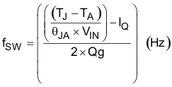
The maximum allowable package power dissipation is related to ambient temperature by Equation 45.

Substituting Equation 38 into Equation 43 and solving for fSW yields the maximum operating frequency for the TPS4005x. The result is described in Equation 46.
