ZHCSJU9E January 2007 – June 2019 TPS40077
PRODUCTION DATA.
- 1 特性
- 2 应用
- 3 说明
- 4 修订历史记录
- 5 Pin Configuration and Functions
- 6 Specifications
-
7 Detailed Description
- 7.1 Overview
- 7.2 Functional Block Diagram
- 7.3
Feature Description
- 7.3.1 Minimum Pulse Duration
- 7.3.2 Slew Rate Limit On VDD
- 7.3.3 Setting The Switching Frequency (Programming The Clock Oscillator)
- 7.3.4 Loop Compensation
- 7.3.5 Shutdown and Sequencing
- 7.3.6 Boost and LVBP Bypass Capacitance
- 7.3.7 Internal Regulators
- 7.3.8 Power Dissipation
- 7.3.9 Boost Diode
- 7.3.10 Synchronous Rectifier Control
- 7.4 Programming
-
8 Application and Implementation
- 8.1 Application Information
- 8.2
Typical Applications
- 8.2.1
Buck Regulator 8-V to 16-V Input, 1.8-V Output at 10 A
- 8.2.1.1 Design Requirements
- 8.2.1.2
Detailed Design Procedure
- 8.2.1.2.1
Power Train Components
- 8.2.1.2.1.1 Output Inductor, LOUT
- 8.2.1.2.1.2 Output Capacitor, COUT, ELCO and MLCC
- 8.2.1.2.1.3 Input Capacitor, CIN ELCO and MLCC
- 8.2.1.2.1.4 Switching MOSFET, QSW
- 8.2.1.2.1.5 Rectifier MOSFET, QSR
- 8.2.1.2.1.6 Timing Resistor, RT
- 8.2.1.2.1.7 Feed-Forward and UVLO Resistor, RKFF
- 8.2.1.2.1.8 Soft-Start Capacitor, CSS
- 8.2.1.2.1.9 Short-Circuit Protection, RILIM and CILIM
- 8.2.1.2.1.10 Boost Voltage, CBOOST and DBOOST (Optional)
- 8.2.1.2.1.11 Closing the Feedback Loop, RZ1, RP1, RPZ2, RSET1, RSET2, CZ2, CP2, and CPZ1
- 8.2.1.2.1
Power Train Components
- 8.2.1.3 Application Curves
- 8.2.1
Buck Regulator 8-V to 16-V Input, 1.8-V Output at 10 A
- 8.3 Additional System Examples
- 9 Layout
- 10器件和文档支持
- 11机械、封装和可订购信息
7.3.5 Shutdown and Sequencing
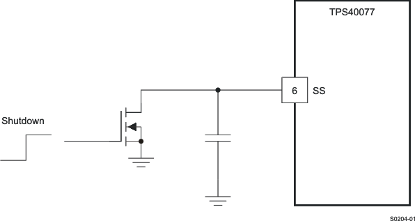
The TPS40077 can be shut down by pulling the SS pin below 250 mV. In this state, both of the output drivers are in the low-output state, turning off both of the power FETs. This places the output of the converter in a high-impedance state. When shutting down the converter, a crisp pulldown of the SS pin is preferred to a slow pulldown. A slow pulldown could allow the output to be pulled low, possibly sinking current from the load. As a general rule of thumb, the fall time of SS when shutting down the converter should be no more than 1/10th of the control loop crossover frequency. An example of a shutdown interface is shown in Figure 23.
 Figure 23. TPS40077 Shutdown
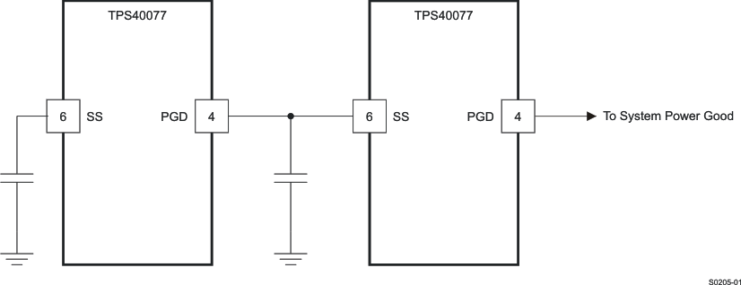
 In a similar manner, power supplies based on the TPS40077 can be sequenced by connecting the PGD pin of the first supply to come up to the SS pin of the second supply as shown in Figure 24.
 Figure 24. TPS40077 Sequencing