ZHCSJU9E January 2007 – June 2019 TPS40077
PRODUCTION DATA.
- 1 特性
- 2 应用
- 3 说明
- 4 修订历史记录
- 5 Pin Configuration and Functions
- 6 Specifications
-
7 Detailed Description
- 7.1 Overview
- 7.2 Functional Block Diagram
- 7.3
Feature Description
- 7.3.1 Minimum Pulse Duration
- 7.3.2 Slew Rate Limit On VDD
- 7.3.3 Setting The Switching Frequency (Programming The Clock Oscillator)
- 7.3.4 Loop Compensation
- 7.3.5 Shutdown and Sequencing
- 7.3.6 Boost and LVBP Bypass Capacitance
- 7.3.7 Internal Regulators
- 7.3.8 Power Dissipation
- 7.3.9 Boost Diode
- 7.3.10 Synchronous Rectifier Control
- 7.4 Programming
-
8 Application and Implementation
- 8.1 Application Information
- 8.2
Typical Applications
- 8.2.1
Buck Regulator 8-V to 16-V Input, 1.8-V Output at 10 A
- 8.2.1.1 Design Requirements
- 8.2.1.2
Detailed Design Procedure
- 8.2.1.2.1
Power Train Components
- 8.2.1.2.1.1 Output Inductor, LOUT
- 8.2.1.2.1.2 Output Capacitor, COUT, ELCO and MLCC
- 8.2.1.2.1.3 Input Capacitor, CIN ELCO and MLCC
- 8.2.1.2.1.4 Switching MOSFET, QSW
- 8.2.1.2.1.5 Rectifier MOSFET, QSR
- 8.2.1.2.1.6 Timing Resistor, RT
- 8.2.1.2.1.7 Feed-Forward and UVLO Resistor, RKFF
- 8.2.1.2.1.8 Soft-Start Capacitor, CSS
- 8.2.1.2.1.9 Short-Circuit Protection, RILIM and CILIM
- 8.2.1.2.1.10 Boost Voltage, CBOOST and DBOOST (Optional)
- 8.2.1.2.1.11 Closing the Feedback Loop, RZ1, RP1, RPZ2, RSET1, RSET2, CZ2, CP2, and CPZ1
- 8.2.1.2.1
Power Train Components
- 8.2.1.3 Application Curves
- 8.2.1
Buck Regulator 8-V to 16-V Input, 1.8-V Output at 10 A
- 8.3 Additional System Examples
- 9 Layout
- 10器件和文档支持
- 11机械、封装和可订购信息
8.2.1.2.1.11 Closing the Feedback Loop, RZ1, RP1, RPZ2, RSET1, RSET2, CZ2, CP2, and CPZ1
A graphical method is used to select the compensation components. This is a standard feed-forward buck converter. Its PWM gain is given by Equation 44.

The ramp voltage is 1 V at the UVLO voltage. Because of the feed-forward compensation, the programmed UVLO voltage is the voltage that sets the PWM gain.
The gain of the output LC filter is given by Equation 45.

The PWM and LC gain is Equation 46.

To plot this on a Bode plot, the dc gain must be expressed in dB. The dc gain is equal to KPWM. To express this in dB, take its logarithm and multiply by 20. For this converter, the dc gain is Equation 47.

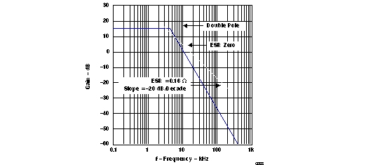
Also, the pole and zero frequencies should be calculated. A double pole is associated with the LC and a zero is associated with the ESR of the output capacitor. The frequencies where these occur can be calculated using Equation 48 and Equation 49.


These are shown in the Bode plot of Figure 29.
 Figure 29. PWM and LC Filter Gain
 The next step is to establish the required compensation gain to achieve the desired overall system response. The target response is to have the crossover frequency between 1/9 and 1/5 times the switching frequency, in order to have a phase margin greater than 45° and a gain margin greater than 6 dB.
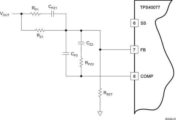
A type-III compensation network, shown in Figure 30, was used for this design. This network gives the best overall flexibility for compensating the converter.
 Figure 30. Type-III Compensation With the TPS40077
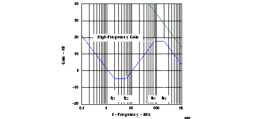
 A typical Bode plot for this type of compensation network is shown in Figure 31.
 Figure 31. Type-III Compensation Typical Bode Plot
 The high-frequency gain and the break (pole and zero) frequencies are calculated using Equation 50 through Equation 55.


Looking at the PWM and LC bode plot, there are a few things which must be done to achieve stability.
- Place two zeros close to the double pole, e.g., fZ1 = fZ2 = 4.3 kHz
- Place both poles well above the crossover frequency. The crossover frequency was selected as one sixth the switching frequency, fco1 = 50 kHz, fP1 = 66 kHz
- Place the second pole at three times fco1. This ensures that the overall system gain falls off quickly to give good gain margin, fp2 = 150 kHz
- The high-frequency gain should be sufficient to ensure 0 dB at the required crossover frequency, GAIN = –1 × gain of PWM and LC at the crossover frequency, GAIN = 16.9 dB
Using these values and Equation 50 through Equation 55, the Rs and Cs around the compensation network can be calculated.
- Set RZ1 = 51 kΩ
- Calculate RSET using Equation 50, RSET = 32.4 kΩ
- Using Equation 54 and fz1 = 4.3 kHz, CPZ1 can be calculated to be 726 pF, CPZ1= 680 pF
- fP1 and Equation 52 yields RP1 to be a standard value of 3.3 kΩ.
- The required gain of 16.9 dB and Equation 51 sets the value for RPZ2. RPZ2 = 21.5 kΩ.
- CZ2 is calculated using Equation 55 and the desired frequency for the second zero, CZ2 = 1.7 nF, or using standard values, 1.8 nF.
- Finally, CP2 is calculated using the second pole frequency and Equation 53; CP2 = 47 pF.
Using these values, the simulated results are 57° of phase margin at 54 kHz.