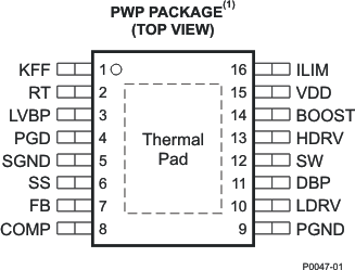
| 1 |
KFF |
I |
A resistor connected from this pin to VIN programs the amount of feed-forward voltage. The current fed into this pin is internally divided by 25 and used to control the slope of the PWM ramp and program UVLO. Nominal voltage at this pin is maintained at 400 mV. |
| 2 |
RT |
I |
A resistor is connected from this pin to ground to set the internal oscillator and switching frequency. |
| 3 |
LVBP |
O |
4.2-V reference used for internal device logic only. This pin should be bypassed by a 0.1-μF ceramic capacitor. External loads that are less than 1 mA and electrically quiet may be applied. |
| 4 |
PGD |
O |
This is an open-drain output that pulls to ground when soft start is active, or when the FB pin is outside a ±10% band around VREF. |
| 5 |
SGND |
— |
Signal ground reference for the device. Low-level quiet circuitry around the IC should connect to this pin. This pin should be connected to the thermal pad under the IC, and that thermal pad should connect to the PGND pin. Do not allow power currents to flow in the thermal pad or in the SGND part of the ground for best results. |
| 6 |
SS |
I |
Soft-start programming pin. A capacitor connected from this pin to GND programs the soft-start time. The capacitor is charged with an internal current source of 12 μA. The resulting voltage ramp on the SS pin is used as a second noninverting input to the error amplifier. The voltage at this error amplifier input is approximately 1 V less than that on the SS pin. Output voltage regulation is controlled by the SS voltage ramp until the voltage on the SS pin reaches the internal offset voltage of 1 V plus the internal reference voltage of 700 mV. If SS is pulled below 225 mV, the device goes into a shutdown state where the power FETSs are turned off and the prebias circuitry is reset. If the programmed UVLO voltage is below 6 V, connect a 330-kΩ resistor in parallel with the SS capacitor. Also provides timing for fault recovery attempts. |
| 7 |
FB |
I |
Inverting input to the error amplifier. In normal operation, the voltage on this pin is equal to the internal reference voltage, 0.7 V. |
| 8 |
COMP |
O |
Output of the error amplifier, input to the PWM comparator. A feedback network is connected from this pin to the FB pin to compensate the overall loop. The COMP pin is internally clamped to 3.4 V. |
| 9 |
PGND |
— |
Power ground reference for the device. There should be a low-impedance path from this pin to the source(s) of the lower MOSFET(s). |
| 10 |
LDRV |
O |
Gate drive for the N-channel synchronous rectifier. This pin switches from DBP (MOSFET on) to ground (MOSFET off). For proper operation, the total gate charge of the MOSFET connected to LDRV should be less than 50 nC. |
| 11 |
DBP |
O |
8-V reference used for the gate drive of the N-channel synchronous rectifier. This pin should be bypassed to ground with a 1-μF ceramic capacitor. |
| 12 |
SW |
I |
This pin is connected to the switched node of the converter. It is used for short-circuit sensing and gate-drive timing information and is the return for the high-side driver. A 1.5-Ω resistor is required in series with this pin for protection against substrate current issues. |
| 13 |
HDRV |
O |
Floating gate drive for the high-side N-channel MOSFET. This pin switches from BOOST (MOSFET on) to SW (MOSFET off). |
| 14 |
BOOST |
I |
The peak voltage on BOOST is equal to the SW node voltage plus the voltage present at DBP less the bootstrap diode drop. This drop can be 1.4 V for the internal bootstrap diode or 300 mV for an external Schottky diode. The voltage differential between this pin and SW is the available drive voltage for the high-side FET. |
| 15 |
VDD |
I |
Supply voltage for the device. |
| 16 |
ILIM |
I |
Short-circuit-protection programming pin. This pin is used to set the short circuit detection threshold. An internal current sink from this pin to ground sets a voltage drop across an external resistor connected from this pin to VDD. The voltage on this pin is compared to the voltage drop (VVDD – VSW) across the high side N-channel MOSFET during conduction. Just prior to the beginning of a switching cycle, this pin is pulled to approximately VDD/2 and released when SW is within 2 V of VDD or after a timeout (the precondition time), whichever occurs first. Placing a capacitor across the resistor from ILIM to VDD allows the ILIM threshold to decrease during the switch-on time, effectively programming the ILIM blanking time. See Application Information. |
