ZHCSH96H MARCH 2007 – May 2019 TPS40192 , TPS40193
PRODUCTION DATA.
- 1 特性
- 2 应用
- 3 说明
- 4 修订历史记录
- 5 Pin Configuration and Functions
- 6 Specifications
- 7 Detailed Description
-
8 Application and Implementation
- 8.1 Application Information
- 8.2
Typical Application
- 8.2.1 Design Requirements
- 8.2.2
Detailed Design Procedure
- 8.2.2.1 Selecting the Switching Frequency
- 8.2.2.2 Inductor Selection
- 8.2.2.3 Output Capacitor Selection (C8)
- 8.2.2.4 Peak Current Rating of the Inductor
- 8.2.2.5 Input Capacitor Selection (C7)
- 8.2.2.6 MOSFET Switch Selection (Q1, Q2)
- 8.2.2.7 Boot Strap Capacitor
- 8.2.2.8 Input Bypass Capacitor (C6)
- 8.2.2.9 BP5 Bypass Capacitor (C5)
- 8.2.2.10 Input Voltage Filter Resistor (R11)
- 8.2.2.11 Short Circuit Protection (R9)
- 8.2.2.12 Feedback Compensation (Modeling the Power Stage)
- 8.2.2.13 Feedback Divider (R7, R8)
- 8.2.2.14 Error Amplifier Compensation (R6, R10, C1, C2, C3)
- 8.2.3 Application Curves
- 9 Power Supply Recommendations
- 10Layout
- 11器件和文档支持
- 12机械、封装和可订购信息
7.3.4 Enable Functionality
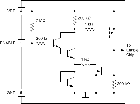
A dedicated ENABLE pin simplifies a user-level interface design where no multiplexed functions exist. Another benefit is a true low power shutdown mode of operation. When the ENABLE pin is pulled to GND, all unnecessary functions, including the BP5 regulator, are turned off, reducing the device supply (IDD) current to 45-µA. A functionally equivalent circuit of the enable circuitry shown in Figure 12.
 Figure 12. Enable Pin Internal Circuitry
 If the ENABLE pin is left floating, the chip starts automatically. The pin must be pulled to less than 600 mV to ensure that the TPS40192 and TPS40193 devices is in shutdown mode. Note that the ENABLE pin is relatively high impedance. Some applications generate enough nearby noise to cause the ENABLE pin to swing below the 600 mV threshold and give an erroneous shutdown commands to the rest of the device. There are two solutions to solve this problem.
- Place a capacitor from ENABLE to GND. A side effect of this is to delay the start of the converter while the capacitor charges past the enable threshold
- Place a resistor from VDD to ENABLE. This causes more current to flow in the shutdown mode, but does not delay converter start-up. If a resistor is used, the total current into the ENABLE pin should be limited to no more than 500 μA.
The ENABLE pin is self-clamping. The clamp voltage can be as low as 1 V with a 1-kΩ ground impedance. Due to this self-clamping feature, the pullup impedance on the ENABLE pin should be selected to limit the sink current to less than 500 µA. Driving the ENABLE pin with a low-impedance source voltage can result in damage to the device. Because of the self-clamping feature, it requires care when connecting multiple ENABLE pins together.