ZHCSH96H MARCH 2007 – May 2019 TPS40192 , TPS40193
PRODUCTION DATA.
- 1 特性
- 2 应用
- 3 说明
- 4 修订历史记录
- 5 Pin Configuration and Functions
- 6 Specifications
- 7 Detailed Description
-
8 Application and Implementation
- 8.1 Application Information
- 8.2
Typical Application
- 8.2.1 Design Requirements
- 8.2.2
Detailed Design Procedure
- 8.2.2.1 Selecting the Switching Frequency
- 8.2.2.2 Inductor Selection
- 8.2.2.3 Output Capacitor Selection (C8)
- 8.2.2.4 Peak Current Rating of the Inductor
- 8.2.2.5 Input Capacitor Selection (C7)
- 8.2.2.6 MOSFET Switch Selection (Q1, Q2)
- 8.2.2.7 Boot Strap Capacitor
- 8.2.2.8 Input Bypass Capacitor (C6)
- 8.2.2.9 BP5 Bypass Capacitor (C5)
- 8.2.2.10 Input Voltage Filter Resistor (R11)
- 8.2.2.11 Short Circuit Protection (R9)
- 8.2.2.12 Feedback Compensation (Modeling the Power Stage)
- 8.2.2.13 Feedback Divider (R7, R8)
- 8.2.2.14 Error Amplifier Compensation (R6, R10, C1, C2, C3)
- 8.2.3 Application Curves
- 9 Power Supply Recommendations
- 10Layout
- 11器件和文档支持
- 12机械、封装和可订购信息
6.7 Typical Characteristics
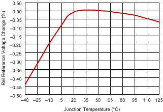 Figure 1. Relative Reference Feedback Voltage vs Junction Temperature
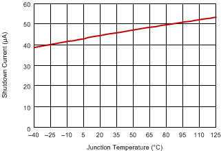
| VENABLE < 0.6 V |
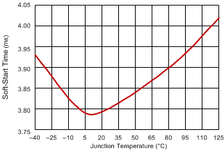 Figure 5. Soft-start Time vs Junction Temperature
 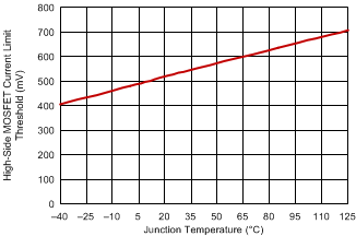 Figure 7. High-Side MOSFET Current Limit Threshold vs Junction Temperature
 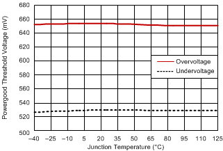 Figure 9. Power-Good Threshold voltage vs Junction Temperature
 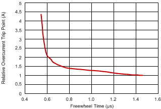 Figure 11. Relative Overcurrent Trip Point vs Freewheel Time
 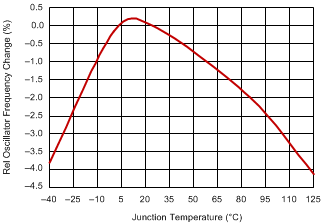 Figure 2. Relative Oscillator Frequency Change vs Junction Temperature
 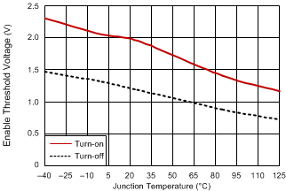 Figure 4. Enable Threshold Voltage vs Junction Temperature
 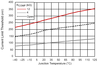 Figure 6. Low-Side MOSFET Current Limit Threshold vs Junction Temperature
 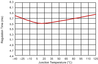 Figure 8. Total Time to Regulation vs Junction Temperature
 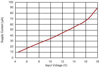 Figure 10. Shutdown Current vs Input Voltage