ZHCSED0 November 2015 TPS40210-EP
PRODUCTION DATA.
- 1 特性
- 2 应用
- 3 说明
- 4 修订历史记录
- 5 Pin Configuration and Functions
- 6 Specifications
-
7 Detailed Description
- 7.1 Overview
- 7.2 Functional Block Diagram
- 7.3
Feature Description
- 7.3.1 Soft-Start
- 7.3.2 BP Regulator
- 7.3.3 Shutdown (DIS/EN Pin)
- 7.3.4 Minimum On-Time and Off-Time Considerations
- 7.3.5 Setting the Oscillator Frequency
- 7.3.6 Synchronizing the Oscillator
- 7.3.7 Current Sense and Overcurrent
- 7.3.8 Current Sense and Subharmonic Instability
- 7.3.9 Current Sense Filtering
- 7.3.10 Control Loop Considerations
- 7.3.11 Gate Drive Circuit
- 7.4 Device Functional Modes
-
8 Application and Implementation
- 8.1 Application Information
- 8.2
Typical Application
- 8.2.1 Design Requirements
- 8.2.2
Detailed Design Procedure
- 8.2.2.1 Duty Cycle Estimation
- 8.2.2.2 Inductor Selection
- 8.2.2.3 Rectifier Diode Selection
- 8.2.2.4 Output Capacitor Selection
- 8.2.2.5 Input Capacitor Selection
- 8.2.2.6 Current Sense and Current Limit
- 8.2.2.7 Current Sense Filter
- 8.2.2.8 Switching MOSFET Selection
- 8.2.2.9 Feedback Divider Resistors
- 8.2.2.10 Error Amplifier Compensation
- 8.2.2.11 RC Oscillator
- 8.2.2.12 Soft-Start Capacitor
- 8.2.2.13 Regulator Bypass
- 8.2.2.14 Bill of Materials
- 8.2.3 Application Curves
- 9 Power Supply Recommendations
- 10Layout
- 11器件和文档支持
- 12机械、封装和可订购信息
6 Specifications
6.1 Absolute Maximum Ratings
over operating free-air temperature range unless otherwise noted(1)| MIN | MAX | UNIT | |||
|---|---|---|---|---|---|
| Input voltage | VDD | –0.3 | 52 | V | |
| RC, SS, FB, DIS/EN | –0.3 | 10 | |||
| ISNS | –0.3 | 8 | |||
| Output voltage | COMP, BP, GDRV | –0.3 | 9 | ||
| TJ | Operating junction temperature | –55 | 150 | °C | |
| Tstg | Storage temperature | –55 | 150 | °C | |
(1) Stresses beyond those listed under Absolute Maximum Ratings may cause permanent damage to the device. These are stress ratings only, and functional operation of the device at these or any other conditions beyond those indicated under Recommended Operating Conditions is not implied. Exposure to absolute-maximum-rated conditions for extended periods may affect device reliability.
6.2 ESD Ratings
| VALUE | UNIT | |||
|---|---|---|---|---|
| V(ESD) | Electrostatic discharge | Human-body model (HBM), per ANSI/ESDA/JEDEC JS-001(1) | ±1500 | V |
| Charged-device model (CDM), per JEDEC specification JESD22-C101(2) | ±1500 | |||
(1) JEDEC document JEP155 states that 500-V HBM allows safe manufacturing with a standard ESD control process.
(2) JEDEC document JEP157 states that 250-V CDM allows safe manufacturing with a standard ESD control process.
6.3 Recommended Operating Conditions
| MIN | MAX | UNIT | ||
|---|---|---|---|---|
| VDD | Input voltage | 4.5 | 52 | V |
| TJ | Operating junction temperature | –55 | 125 | °C |
6.4 Thermal Information
| THERMAL METRIC(1) | TPS40210-EP | UNIT | |
|---|---|---|---|
| DRC (VSON) | |||
| 10 PINS | |||
| RθJA | Junction-to-ambient thermal resistance | 67.2 | °C/W |
| RθJC(top) | Junction-to-case (top) thermal resistance | 50.5 | °C/W |
| RθJB | Junction-to-board thermal resistance | 41.0 | °C/W |
| ψJT | Junction-to-top characterization parameter | 2.4 | °C/W |
| ψJB | Junction-to-board characterization parameter | 40.7 | °C/W |
| RθJC(bot) | Junction-to-case (bottom) thermal resistance | 15.6 | °C/W |
(1) For more information about traditional and new thermal metrics, see the Semiconductor and IC Package Thermal Metrics application report, SPRA953.
6.5 Electrical Characteristics
TJ = –55°C to 125°C, VDD= 12Vdc, all parameters at zero power dissipation (unless otherwise noted)| PARAMETER | TEST CONDITIONS | MIN | TYP | MAX | UNIT | |||
|---|---|---|---|---|---|---|---|---|
| VOLTAGE REFERENCE | ||||||||
| VFB | Feedback voltage range | COMP = FB, 4.5 ≤ VDD ≤ 52 V, TJ = 25°C | 693 | 700 | 707 | mV | ||
| COMP = FB, 4.5 ≤ VDD ≤ 52 V, –55°C ≤ TJ ≤ 125°C | 686 | 700 | 714 | |||||
| INPUT SUPPLY | ||||||||
| VDD | Input voltage range | 4.5 | 52 | V | ||||
| IDD | Operating current | 4.5 ≤ VDD ≤ 52 V, no switching, VDIS < 0.8 | 1.5 | 2.5 | mA | |||
| 2.5 ≤ VDIS ≤ 7 V | 10 | 20 | μA | |||||
| VDD < VUVLO(on), VDIS < 0.8 | 530 | μA | ||||||
| UNDERVOLTAGE LOCKOUT | ||||||||
| VUVLO(on) | Turn on threshold voltage | 4.00 | 4.25 | 4.50 | V | |||
| VUVLO(hyst) | UVLO hysteresis | 140 | 195 | 240 | mV | |||
| OSCILLATOR | ||||||||
| ƒOSC | Oscillator frequency range(1) | 35 | 1000 | kHz | ||||
| Oscillator frequency | RRC = 182 kΩ, CRC = 330 pF | 260 | 300 | 340 | ||||
| Frequency line regulation | 4.5 ≤ VDD ≤ 52 V | -20% | 7% | |||||
| VSLP | Slope compensation ramp | 520 | 620 | 720 | mV | |||
| PWM | ||||||||
| tON(min) | Minimum pulse width | VDD = 12 V(1) | 275 | 400 | ns | |||
| VDD = 30 V | 90 | 200 | ||||||
| tOFF(min) | Minimum off time | 170 | 200 | |||||
| VVLY | Valley voltage | 1.2 | V | |||||
| SOFT-START | ||||||||
| VSS(ofst) | Offset voltage from SS pin to error amplifier input | 700 | mV | |||||
| RSS(chg) | Soft-start charge resistance | 320 | 430 | 620 | kΩ | |||
| RSS(dchg) | Soft-start discharge resistance | 840 | 1200 | 1600 | ||||
| ERROR AMPLIFIER | ||||||||
| GBWP | Unity gain bandwidth product(1) | 1.5 | 3.0 | MHz | ||||
| AOL | Open loop gain(1) | 60 | 80 | dB | ||||
| IIB(FB) | Input bias current (current out of FB pin) | 100 | 300 | nA | ||||
| ICOMP(src) | Output source current | VFB = 0.6 V, VCOMP = 1 V | 100 | 250 | μA | |||
| ICOMP(snk) | Output sink current | VFB = 1.2 V, VCOMP = 1 V | 1.2 | 2.5 | mA | |||
| OVERCURRENT PROTECTION | ||||||||
| VISNS(oc) | Overcurrent detection threshold (at ISNS pin) | 4.5 ≤ VDD < 52 V, –55°C ≤ TJ ≤ 125°C | 120 | 150 | 180 | mV | ||
| DOC | Overcurrent duty cycle(1) | 2% | ||||||
| VSS(rst) | Overcurrent reset threshold voltage (at SS pin) | 100 | 150 | 350 | mV | |||
| TBLNK | Leading edge blanking(1) | 75 | ns | |||||
| CURRENT SENSE AMPLIFIER | ||||||||
| ACS | Current sense amplifier gain | 4..2 | 5.6 | 7.4 | V/V | |||
| IB(ISNS) | Input bias current | 1 | 3 | μA | ||||
| DRIVER | ||||||||
| IGDRV(src) | Gate driver source current | VGDRV = 4 V, TJ = 25°C | 375 | 400 | mA | |||
| IGDRV(snk) | Gate driver sink current | VGDRV = 4 V, TJ = 25°C | 330 | 400 | ||||
| LINEAR REGULATOR | ||||||||
| VBP | Bypass voltage output | 0 mA < IBP < 15 mA | 7 | 8 | 9 | V | ||
| DISABLE/ENABLE | ||||||||
| VDIS(en) | Turn-on voltage | 0.7 | 1.3 | V | ||||
| VDIS(hys) | Hysteresis voltage | 25 | 130 | 220 | mV | |||
| RDIS | DIS pin pulldown resistance | 0.7 | 1.1 | 1.6 | MΩ | |||
(1) Ensured by design. Not production tested.
6.6 Typical Characteristics
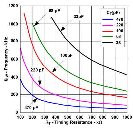 Figure 1. Frequency vs Timing Resistance
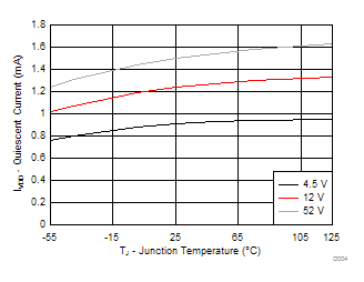
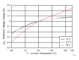
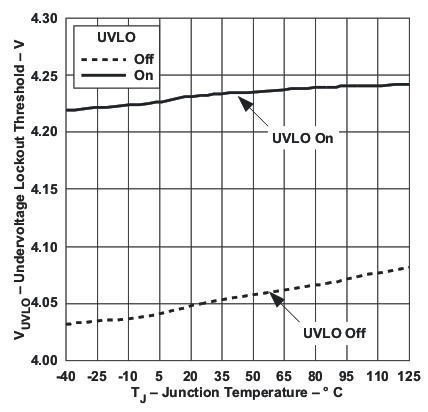 Figure 7. Undervoltage Lockout Threshold vs Junction Temperature
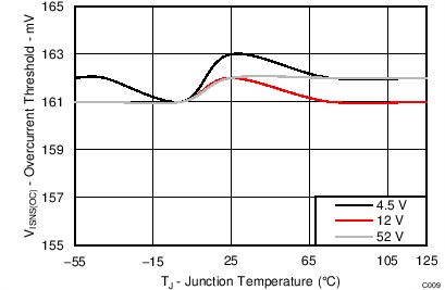
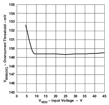 Figure 9. Overcurrent Threshold vs Input Voltage
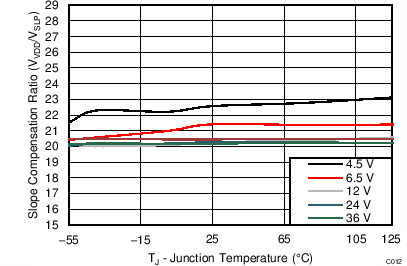
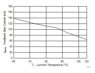
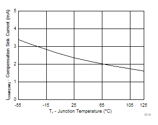
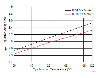
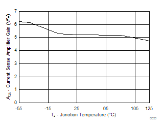
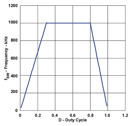 Figure 2. Switching Frequency vs Duty Cycle
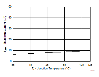
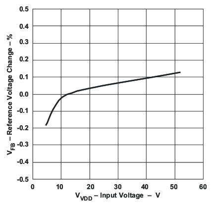 Figure 6. Reference Voltage Change vs Input Voltage
